

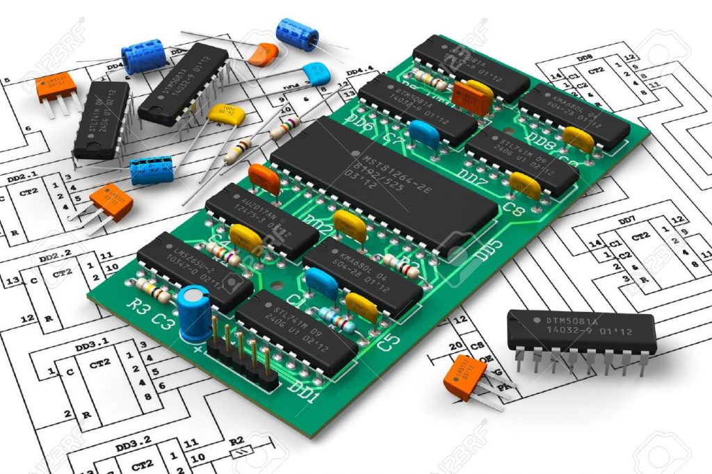
PCB Board Reverse Engineering Network Sytem
PCB Board Reverse Engineering Network Sytem is playing an extremely important role for PCB reverse engineering, in the CAD system, the PCB recovered layout file and gerber file is determined by the network. If the network grid is too dense, although the through way will increase.
But the stepper grid is too small which will significantly give rise to the data processing quantity of image, so in the process of PCB Board Reproducing, it will require the storage area has a much larger space to undertake the requirement. At the same time, it will greatly affect the processor operation speed on the electronic products such as the personal computer.
And some of the through line is invalid, such as the through hole on the edge for alignment and fixture, tooling holes, etc. on the contrary, if the density of network grid is too thin with too few through lines which will have a negative effect. So it is quite critical to have a network system with proper density to support the PCB Board layout;
The standard distance among the component leads is 0.1 inch around 2.54mm, so the basic standard for network grid system is 0.1 inch or 0.05, 0.025, and 0.02inch.
Tags: pcb board reverse engineering,pcb card reverse engineering,pcb circuit board reverse engineering,pcb reverse engineering,pcba reverse engineering,Printed Circuit Board Reverse Engineering,printed wiring board reverse engineering,pwb reverse engineering,pwba reverse engineering