"Everything we build starts with design engineering. CECL manufactured boards for one of our products. It went perfectly – a real success.It is really an high quality service they have provided to us!"
By Nile Smith from Sinotech Inc.
“We had several very old device with obsolete boards need to be replaced –through CECL professional service.We got what we needed, and we’ve been using the results of the work without any problem till now.”
By Richard Anderson from TWP system Inc.
"Guys from CECL manufacture PCBs we use in one of our products, a clinometer and we’ve never had a problem with anything. The boards come in, they work. And, their team is very responsive."
La reconstitution de la structure des circuits imprimés par rétro-ingénierie contribue directement à la préparation de la production et à la fiabilité à long terme. Une fois la structure correctement reconstituée, les ingénieurs peuvent générer des données de fabrication précises et valider la conception par des tests de prototypes. Le circuit imprimé reproduit peut ensuite être évalué en conditions réelles d’utilisation, notamment sous charge électrique, contraintes environnementales et interférences électromagnétiques. Pour les engins de chantier et de terrassement, où les temps d’arrêt sont coûteux et la sécurité primordiale, il est essentiel de garantir que le circuit imprimé d’E/S de l’automate programmable fonctionne de manière identique à l’original. En se concentrant sur la reconstitution de la structure lors de la rétro-ingénierie, les entreprises peuvent remettre à neuf et maintenir en toute confiance les composants électroniques de contrôle critiques, prolongeant ainsi la durée de vie des équipements et assurant une performance d’automatisation stable dans les environnements industriels exigeants.
Die Reverse-Engineering-Methode für den Lagenaufbau von Leiterplatten trägt direkt zur Produktionsreife und langfristigen Zuverlässigkeit bei. Sobald der Lagenaufbau korrekt wiederhergestellt ist, können Ingenieure präzise Fertigungsdaten generieren und das Design durch Prototypentests validieren. Die reproduzierte Leiterplatte kann anschließend unter realen Betriebsbedingungen, einschließlich elektrischer Last, Umwelteinflüssen und elektromagnetischer Störungen, evaluiert werden. Bei schweren Baumaschinen und Erdbewegungsgeräten, wo Ausfallzeiten kostspielig und Sicherheit von entscheidender Bedeutung sind, ist es unerlässlich, dass die SPS-I/O-Leiterplatte identisch zum Original funktioniert. Durch die Fokussierung auf die Rekonstruktion des Lagenaufbaus im Rahmen des Reverse Engineerings können Unternehmen kritische Steuerungselektronik zuverlässig nachfertigen und warten, die Lebensdauer der Geräte verlängern und eine stabile Automatisierungsleistung in anspruchsvollen Industrieumgebungen gewährleisten.
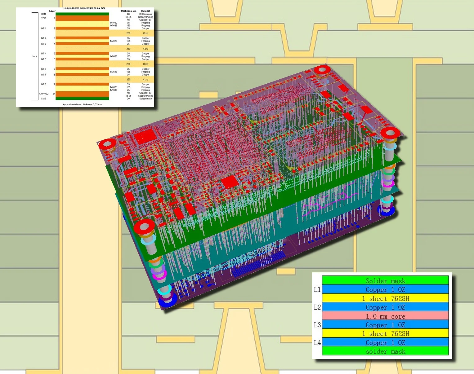
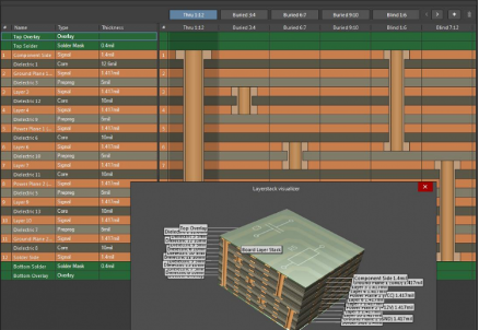
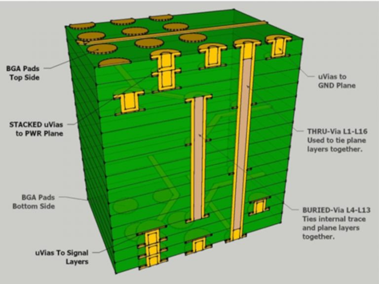
PCB Board Reverse Engineering Lay-Up structure will normally use P as the reference plane layer, S as the signal layer, T as top layer, B as bottom layer. Hereby we would like to take a PCB board with twelve layers as reference to illustrate the structure, and the layer distribution according to their functionality can be seen below:
T-P-S-P-S-P-S-P-S-P-S-S-P-B
PCB Board Reverse Engineering Lay-Up structure will normally use P as the reference plane layer, S as the signal layer, T as top layer, B as bottom layer
Designate the 2nd layer as the high speed digital component power source; use 4th layer as high speed digital ground; but place the decoupling power supply place on top of the PCB board layer, which will be viewed as a reasonable design structure for multilayer PCB board lay-up. Besides, need to ensure the signal circuit drive by same high speed generator and use the same power supply layer as reference plane for PCB reverse engineering, and use this power supply layer as the high speed part source.
La ricostruzione della stratificazione dei circuiti stampati (PCB) tramite reverse engineering contribuisce direttamente alla prontezza produttiva e all’affidabilità a lungo termine. Una volta ripristinata correttamente la stratificazione, gli ingegneri possono generare dati di produzione accurati e convalidare il progetto attraverso test su prototipo. Il PCB riprodotto può quindi essere valutato in condizioni operative reali, tra cui carico elettrico, stress ambientale e interferenze elettromagnetiche. Per le macchine edili e movimento terra, dove i tempi di inattività sono costosi e la sicurezza è fondamentale, è essenziale garantire che il PCB I/O del PLC abbia prestazioni identiche all’originale. Concentrandosi sulla ricostruzione della stratificazione durante il reverse engineering, le aziende possono riprodurre e manutenere con sicurezza l’elettronica di controllo critica, prolungando la durata utile delle apparecchiature e garantendo prestazioni di automazione stabili in ambienti industriali esigenti.
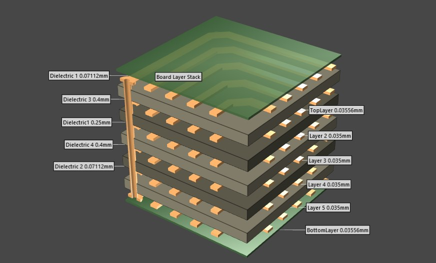
Another critical aspect of PCB lay-up in reverse engineering is its influence on grounding and power distribution strategies. In PLC I/O boards, multiple voltage domains and isolated channels are common, requiring careful separation of analog ground, digital ground, and power return paths. The original lay-up often includes dedicated planes or split regions to control current flow and reduce ground loops. When engineers recreate the layout, preserving these structures is essential to maintain stable operation. Additionally, the lay-up determines thermal dissipation capabilities, which is crucial when the board is installed in sealed enclosures exposed to high ambient temperatures. Reverse engineering that incorporates accurate lay-up reconstruction allows for reliable reproduction, refurbishment, or even controlled redesign to improve manufacturability without compromising performance.
La ingeniería inversa de la disposición de capas de las placas de circuito impreso (PCB) contribuye directamente a la preparación para la producción y a la fiabilidad a largo plazo. Una vez restaurada correctamente la disposición de capas, los ingenieros pueden generar datos de fabricación precisos y validar el diseño mediante pruebas de prototipos. La PCB reproducida puede evaluarse en condiciones de funcionamiento reales, incluyendo carga eléctrica, estrés ambiental e interferencias electromagnéticas. En maquinaria pesada de construcción y movimiento de tierras, donde el tiempo de inactividad es costoso y la seguridad es fundamental, es esencial garantizar que la PCB de E/S del PLC funcione de forma idéntica a la original. Al centrarse en la reconstrucción de la disposición de capas durante la ingeniería inversa, las organizaciones pueden remanufacturar y mantener con confianza la electrónica de control crítica, prolongando la vida útil del equipo y garantizando un rendimiento de automatización estable en entornos industriales exigentes.
PCB kartının tersine mühendislik yöntemiyle katman diziliminin yeniden oluşturulması, üretim hazırlığına ve uzun vadeli güvenilirliğe doğrudan katkıda bulunur. Katman dizilimi doğru bir şekilde yeniden oluşturulduktan sonra, mühendisler doğru üretim verileri üretebilir ve prototip testleri yoluyla tasarımı doğrulayabilirler. Yeniden üretilen PCB daha sonra elektrik yükü, çevresel stres ve elektromanyetik girişim dahil olmak üzere gerçek çalışma koşulları altında değerlendirilebilir. Arıza süresinin maliyetli olduğu ve güvenliğin kritik olduğu ağır inşaat ve hafriyat ekipmanlarında, PLC I/O PCB’sinin orijinaliyle aynı performansı göstermesi çok önemlidir. Tersine mühendislik sırasında katman diziliminin yeniden oluşturulmasına odaklanarak, kuruluşlar kritik kontrol elektroniğini güvenle yeniden üretebilir ve bakımını yapabilir, ekipman ömrünü uzatabilir ve zorlu endüstriyel ortamlarda istikrarlı otomasyon performansı sağlayabilirler.