

PCB Board Circuitry Reverse Engineering Technique
PCB Board Circuitry Reverse Engineering Technique used when the accuracy and resolution of the AD converter increase; Initially, analog-to-digital (A/D) converters originated from the analog paradigm, where most of the physical silicon is analog.
With the development of pcb board reverse engineering topologies, this paradigm evolved into a low-speed A/D converter where digital occupies the main part. Although the A/D converter chip is dominated by analog to dominated by digital, the PCB layout design guidelines have not changed.
When wiring designers reverse engineering mixed-signal circuit boards, they still need key wiring knowledge to achieve effective wiring. This article will take the successive approximation type A/D converter and the ∑-△ type A/D converter as examples to discuss the PCB layout strategy required by the A/D converter
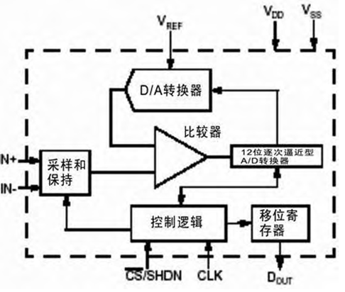
The block diagram of a 12-bit CMOS successive approximation A/D converter. This converter uses the charge distribution formed by the capacitor array.
The successive approximation type A/D converter, regardless of its resolution, usually has at least two ground connections: AGND and DGND. Take Microchip’s A/D converters MCP4008 and MCP3001 as examples here
For high-resolution successive approximation A/D converters, the power and ground of the converter should be connected to the analog plane. Then, the digital output of the A/D converter should be buffered using an external three-state output buffer. In addition to the high drive capability, these buffers also have the function of isolating the analog and digital sides