"Everything we build starts with design engineering. CECL manufactured boards for one of our products. It went perfectly – a real success.It is really an high quality service they have provided to us!"
By Nile Smith from Sinotech Inc.
“We had several very old device with obsolete boards need to be replaced –through CECL professional service.We got what we needed, and we’ve been using the results of the work without any problem till now.”
By Richard Anderson from TWP system Inc.
"Guys from CECL manufacture PCBs we use in one of our products, a clinometer and we’ve never had a problem with anything. The boards come in, they work. And, their team is very responsive."
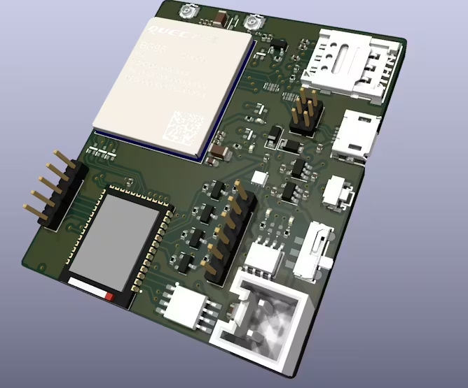
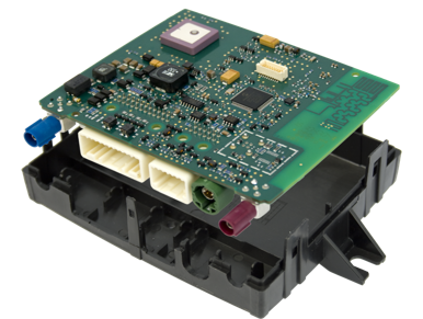
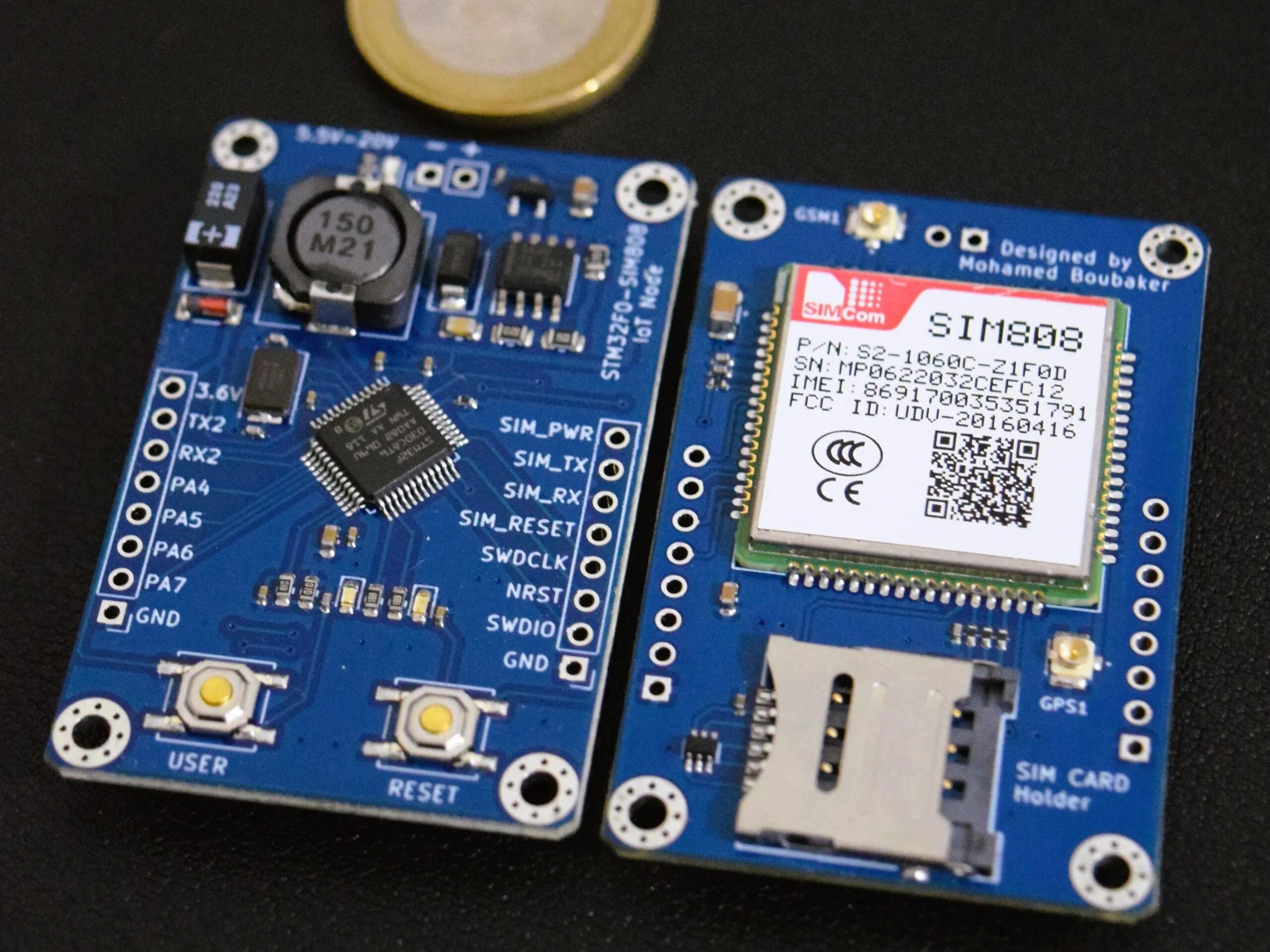
PC Board Reverse Engineering Principle defines a systematic methodology for understanding, restoring, and reproducing complex electronic designs when original engineering data is unavailable. This principle is especially valuable for GPS Tracking & Telematics Modules used in excavators, where reliable monitoring of vehicle location, operating status, and performance data is essential for fleet management and remote diagnostics.
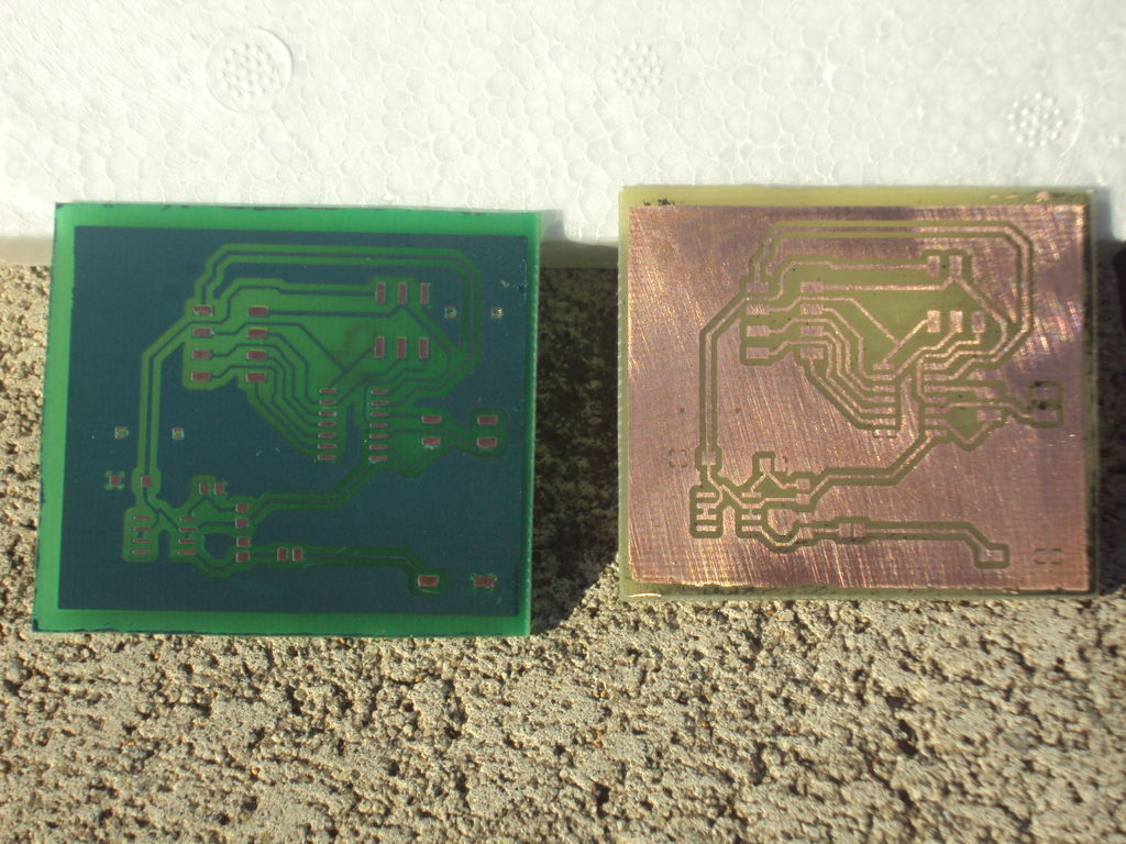
Il processo di reverse engineering inizia con un’ispezione completa del circuito stampato (PCB) esistente. Gli ingegneri analizzano la scheda nuda per ricostruire la topologia del circuito, identificando i blocchi funzionali come i ricevitori GNSS, i moduli di comunicazione cellulare, i circuiti di regolazione dell’alimentazione e le interfacce del microcontrollore. Tracciando i percorsi dei segnali e le interconnessioni dei componenti, è possibile ricostruire gradualmente lo schema elettrico originale, ottenendo una visione chiara del flusso del segnale RF, della logica di elaborazione dei dati e delle strategie di gestione dell’alimentazione. Questa fase è fondamentale per comprendere come i dati di posizionamento e le informazioni di telemetria vengono acquisiti e trasmessi. Una volta chiarita la logica elettrica, viene ricreato il progetto fisico. La struttura dei layer, il percorso delle tracce, il controllo dell’impedenza e i metodi di messa a terra vengono documentati per generare disegni di layout, file Gerber e dati di netlist precisi. Questi elementi consentono di copiare, clonare o replicare il PCB con elevata fedeltà. Durante questa fase, gli ingegneri possono riprogettare selettivamente aree specifiche per migliorare l’integrità del segnale, le prestazioni termiche o la compatibilità elettromagnetica, preservando al contempo la funzionalità originale.
PC Board Reverse Engineering Principle will include the processing procedures, design rules and inspection rules, notes needs to be taken when reverse engineering circuit card. etc;
PC Board Reverse Engineering Principle will include the processing procedures, design rules and inspection rules, notes needs to be taken when reverse engineering circuit card. etc
Reverse engineering a PC Board needs to go through below steps and each one of them has the rules to follow, generally speaking, reverse engineering electronic circuit board need to undergo three big steps:
First of all, pc board schematic diagram design: it is mainly designed by a PROTEL99 schematic design system (advanced schematic) to restore a pc board schematic diagram. During this process, we should take full advantage of all the schematic diagram preparation tools provided by Protel99, and various editing functions to realize our purpose for a correct, and beautiful PC board schematic diagram.
Tersine mühendislik süreci, mevcut PCB’nin kapsamlı bir incelemesiyle başlar. Mühendisler, devre topolojisini kurtarmak, GNSS alıcıları, hücresel iletişim modülleri, güç regülasyonu ve mikrodenetleyici arayüzleri gibi fonksiyonel blokları belirlemek için çıplak kartı analiz ederler. Sinyal yollarını ve bileşen bağlantılarını izleyerek, orijinal şematik diyagram kademeli olarak geri yüklenebilir ve RF sinyal akışı, veri işleme mantığı ve güç yönetimi stratejileri hakkında görünürlük sağlanabilir. Bu adım, konumlandırma verilerinin ve telemetri bilgilerinin nasıl yakalanıp iletildiğini anlamak için kritik öneme sahiptir. Elektriksel mantık netleştirildikten sonra, fiziksel tasarım yeniden oluşturulur. Katman yapısı, iz yönlendirmesi, empedans kontrolü ve topraklama yöntemleri, doğru yerleşim çizimi, Gerber dosyası ve netlist verileri oluşturmak için belgelenir. Bu çıktılar, PCB’nin yüksek doğrulukla kopyalanmasını, klonlanmasını veya çoğaltılmasını mümkün kılar. Bu aşamada, mühendisler orijinal işlevselliği korurken sinyal bütünlüğünü, termal performansı veya elektromanyetik uyumluluğu iyileştirmek için belirli alanları seçici olarak yeniden tasarlayabilirler.
Component analysis follows documentation recovery. A verified BOM list is established by identifying part numbers, electrical ratings, and package types. When components are obsolete or difficult to source, equivalent substitutes are evaluated, allowing the design to be refurbished through controlled redevelopment. This ensures that the reproduced board remains manufacturable without compromising performance or reliability.
Secondly it is generate the network list, netlist is a bridge between the design of pc board schematic diagram and pc board circuit diagram restoration, it has also been called the soul of pcb card cloning. Netlist can be obtained from pc board schematic diagram or from the extraction of pc board physical sample;
Third, pc board reverse engineering is mainly focusing on the other important part of printed circuit board design. In this process we will use protel99 to reverse engineering pcb and fulfill the difficult task.
How to design and draw a simple schematic diagram of pc board
Der Reverse-Engineering-Prozess beginnt mit einer umfassenden Inspektion der vorhandenen Leiterplatte. Ingenieure analysieren die unbestückte Platine, um die Schaltungstopologie zu rekonstruieren und funktionale Blöcke wie GNSS-Empfänger, Mobilfunkmodule, Spannungsregler und Mikrocontroller-Schnittstellen zu identifizieren. Durch die Verfolgung von Signalwegen und Komponentenverbindungen kann der ursprüngliche Schaltplan schrittweise wiederhergestellt werden, wodurch Einblicke in den HF-Signalfluss, die Datenverarbeitungslogik und die Energieverwaltungsstrategien gewonnen werden. Dieser Schritt ist entscheidend, um zu verstehen, wie Positionsdaten und Telemetrieinformationen erfasst und übertragen werden. Sobald die elektrische Logik geklärt ist, wird das physikalische Design rekonstruiert. Schichtaufbau, Leiterbahnführung, Impedanzkontrolle und Erdungsmethoden werden dokumentiert, um eine präzise Layoutzeichnung, Gerber-Dateien und Netzlistendaten zu erstellen. Diese Ergebnisse ermöglichen es, die Leiterplatte originalgetreu zu kopieren, zu klonen oder zu reproduzieren. In dieser Phase können Ingenieure gezielt bestimmte Bereiche neu gestalten, um die Signalintegrität, die thermische Leistung oder die elektromagnetische Verträglichkeit zu verbessern, ohne die ursprüngliche Funktionalität zu beeinträchtigen.
When we design and draw a pc board schematic diagram, below process can be followed to ensure a good schematic diagram being made:
First of all, the size of design paper should adapt to the schematic diagram size after being drawed by PROTEL99, we need to figure out the electronic components and design the paper size. Paper size is determined by the schematic diagram’s dimension and complexity level.
Second step is installation of pc board reverse engineering environment, this process include the set up of grid size and type, cursor type. Etc. most of the parameters can use the systematic default value.
Le processus de rétro-ingénierie commence par une inspection approfondie du circuit imprimé existant. Les ingénieurs analysent la carte nue pour reconstituer la topologie du circuit et identifier les blocs fonctionnels tels que les récepteurs GNSS, les modules de communication cellulaire, les circuits de régulation d’alimentation et les interfaces de microcontrôleur. En retraçant les chemins des signaux et les interconnexions des composants, le schéma électrique d’origine peut être progressivement reconstitué, ce qui permet de visualiser le flux des signaux RF, la logique de traitement des données et les stratégies de gestion de l’alimentation. Cette étape est cruciale pour comprendre comment les données de positionnement et les informations de télémétrie sont capturées et transmises. Une fois la logique électrique clarifiée, la conception physique est recréée. La structure des couches, le routage des pistes, le contrôle d’impédance et les méthodes de mise à la terre sont documentés afin de générer un schéma de câblage précis, un fichier Gerber et une liste de connexions. Ces éléments permettent de copier, cloner ou reproduire le circuit imprimé avec une grande fidélité. Au cours de cette phase, les ingénieurs peuvent redessiner certaines zones spécifiques pour améliorer l’intégrité du signal, les performances thermiques ou la compatibilité électromagnétique, tout en préservant la fonctionnalité d’origine.
Third step is rotating the component: fetch the components out from the component library and put it right now the paper for definition and installation when pc board reverse engineering.
4th step is use tools provided by PROTEL 99se to compile the schematic diagram, and connect each one of the components on the drawing together by meaningful track and simbols to compile a complete schematic diagram;
रिवर्स इंजीनियरिंग प्रोसेस मौजूदा PCB के पूरे इंस्पेक्शन से शुरू होता है। इंजीनियर सर्किट टोपोलॉजी को रिकवर करने, GNSS रिसीवर, सेलुलर कम्युनिकेशन मॉड्यूल, पावर रेगुलेशन और माइक्रोकंट्रोलर इंटरफेस जैसे फंक्शनल ब्लॉक की पहचान करने के लिए बेयर बोर्ड को एनालाइज़ करते हैं। सिग्नल पाथ और कंपोनेंट इंटरकनेक्शन को ट्रेस करके, ओरिजिनल स्कीमैटिक डायग्राम को धीरे-धीरे रिस्टोर किया जा सकता है, जिससे RF सिग्नल फ्लो, डेटा प्रोसेसिंग लॉजिक और पावर मैनेजमेंट स्ट्रेटेजी की विज़िबिलिटी मिलती है। यह स्टेप यह समझने के लिए ज़रूरी है कि पोजिशनिंग डेटा और टेलीमेट्री जानकारी कैसे कैप्चर और ट्रांसमिट की जाती है। एक बार इलेक्ट्रिकल लॉजिक क्लियर हो जाने के बाद, फिजिकल डिज़ाइन को फिर से बनाया जाता है। लेयर स्ट्रक्चर, ट्रेस रूटिंग, इम्पीडेंस कंट्रोल और ग्राउंडिंग मेथड को डॉक्यूमेंट किया जाता है ताकि सटीक लेआउट ड्राइंग, Gerber फ़ाइल और नेटलिस्ट डेटा जेनरेट किया जा सके। ये डिलिवरेबल्स PCB को हाई फिडेलिटी के साथ कॉपी, क्लोन या रेप्लिकेट करना मुमकिन बनाते हैं। इस फेज़ के दौरान, इंजीनियर ओरिजिनल फंक्शनैलिटी को बनाए रखते हुए सिग्नल इंटीग्रिटी, थर्मल परफॉर्मेंस या इलेक्ट्रोमैग्नेटिक कम्पैटिबिलिटी को बेहतर बनाने के लिए खास एरिया को चुनकर रीडिज़ाइन कर सकते हैं।
The primary usage of PC Board Reverse Engineering Principle is extending product life cycles, maintaining legacy telematics systems, and enabling localized manufacturing. However, difficulties may arise from multilayer RF designs, encrypted communication interfaces, or tight tolerance requirements. Addressing these challenges requires experience, precise measurement, and disciplined validation procedures.
When applied correctly, this principle transforms a single existing PCB into a complete, production-ready engineering asset, ensuring continuity and control over critical GPS tracking and telematics solutions.