"Everything we build starts with design engineering. CECL manufactured boards for one of our products. It went perfectly – a real success.It is really an high quality service they have provided to us!"
By Nile Smith from Sinotech Inc.
“We had several very old device with obsolete boards need to be replaced –through CECL professional service.We got what we needed, and we’ve been using the results of the work without any problem till now.”
By Richard Anderson from TWP system Inc.
"Guys from CECL manufacture PCBs we use in one of our products, a clinometer and we’ve never had a problem with anything. The boards come in, they work. And, their team is very responsive."
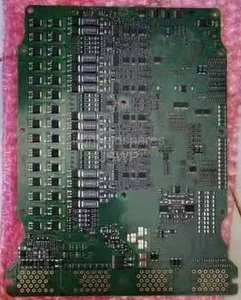
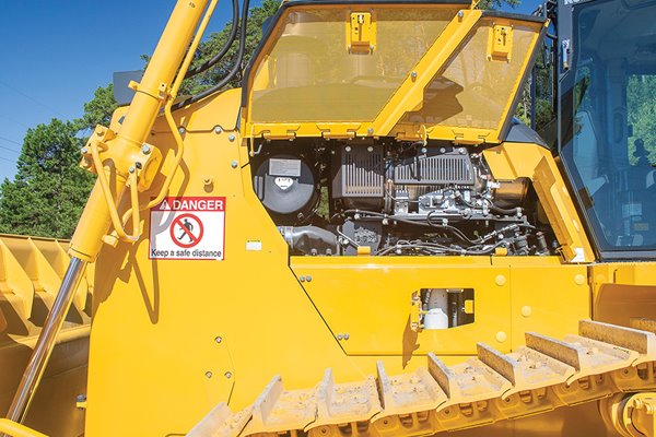
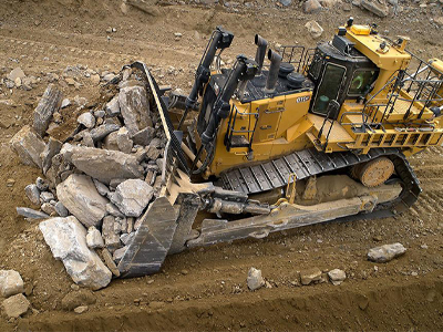
Il reverse engineering di una scheda PC utilizzata nell’unità di controllo motore (ECU) di un bulldozer è un processo tecnico sistematico volto a recuperare, ripristinare e comprendere appieno il progetto elettronico originale che monitora il regime del motore, la coppia erogata e il controllo dell’iniezione di carburante. Il principio inizia con un’analisi completa della scheda fisica, inclusi la struttura dei livelli, i materiali e i vincoli di integrità del segnale. Attraverso metodi di reverse engineering professionali, gli ingegneri possono estrarre i dati del file Gerber dalla scheda PCB originale dell’ECU, ricostruire il disegno del layout e identificare i blocchi funzionali chiave come la gestione dell’alimentazione, le interfacce dei sensori e le unità del microcontrollore. Questo passaggio fondamentale consente operazioni di copia, clonazione o replica accurate, preservando al contempo le prestazioni elettriche originali e la robustezza ambientale richieste per il funzionamento di un bulldozer per impieghi gravosi. Una fase fondamentale del reverse engineering dell’ECU prevede la conversione della scheda fisica in documentazione di progetto digitale. Scansione ad alta risoluzione, separazione strato per strato e net tracing vengono applicati per ricreare con precisione lo schema elettrico e la netlist. Durante questa fase, gli ingegneri riproducono ogni percorso del segnale relativo al rilevamento del regime del motore, al calcolo della coppia e alla fasatura dell’iniezione di carburante. Viene quindi generata una distinta base verificata identificando tutti i componenti attivi e passivi, inclusi i circuiti integrati di livello automobilistico e i dispositivi di protezione. Questo denso processo di ricostruzione consente di riprodurre o rigenerare fedelmente la scheda ECU originale, supportando attività come il ricondizionamento, la duplicazione della produzione o la fornitura di ricambi a lungo termine laddove i produttori originali non forniscano più supporto.
A core stage of ECU reverse engineering involves converting the physical board into digital design documentation. High-resolution scanning, layer-by-layer separation, and net tracing are applied to recreate the schematic diagram and netlist with precision. During this phase, engineers reproduce every signal path related to engine speed sensing, torque calculation, and fuel injection timing. A verified bom list is then generated by identifying all active and passive components, including automotive-grade ICs and protection devices. This dense reconstruction process allows the original ECU board to be faithfully reproduced or remanufactured, supporting tasks such as refurbishment, duplicate production, or long-term spare part supply where original manufacturers no longer provide support.
La rétro-ingénierie d’une carte électronique utilisée dans le calculateur moteur (ECU) d’un bulldozer est un processus technique systématique visant à récupérer, restaurer et comprendre pleinement la conception électronique d’origine qui contrôle le régime moteur, le couple et l’injection de carburant. Le principe repose sur une analyse complète de la carte physique, incluant la structure des couches, les matériaux et les contraintes d’intégrité du signal. Grâce à des méthodes de rétro-ingénierie professionnelles, les ingénieurs peuvent extraire les données Gerber de la carte électronique d’origine de l’ECU, reconstituer le schéma d’implantation et identifier les blocs fonctionnels clés tels que la gestion de l’alimentation, les interfaces des capteurs et les microcontrôleurs. Cette étape fondamentale permet des opérations de copie, de clonage ou de réplication précises, tout en préservant les performances électriques et la robustesse environnementale requises pour le fonctionnement d’un bulldozer. Une étape essentielle de la rétro-ingénierie d’un ECU consiste à convertir la carte physique en documentation de conception numérique. La numérisation haute résolution, la séparation couche par couche et le traçage des connexions sont utilisés pour recréer le schéma et la netlist avec précision. Durant cette phase, les ingénieurs reproduisent chaque chemin de signal lié à la détection du régime moteur, au calcul du couple et au calage de l’injection de carburant. Une nomenclature vérifiée est ensuite générée en identifiant tous les composants actifs et passifs, y compris les circuits intégrés automobiles et les dispositifs de protection. Ce processus de reconstruction précis permet de reproduire ou de remanufacturer fidèlement la carte ECU d’origine, facilitant ainsi des opérations telles que la remise à neuf, la production de copies ou la fourniture de pièces détachées à long terme lorsque les fabricants d’origine ne prennent plus en charge le support.
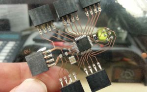
PC Board Reverse Engineering principle needs to go through below steps and each one of them has the rules to follow, generally speaking, reverse engineering PC Board need to undergo three big steps:
Принцип клонування друкованої плати потрібно пройти наведені нижче кроки, і кожен із них має правила, яких слід дотримуватися. Загалом, зворотне проектування PC Board має пройти три великі кроки
Das Reverse Engineering einer Leiterplatte in einem Motorsteuergerät (ECU) eines Bulldozers ist ein systematischer technischer Prozess zur Wiederherstellung und zum vollständigen Verständnis des ursprünglichen elektronischen Designs, das Motordrehzahl, Drehmoment und Kraftstoffeinspritzung steuert. Der Prozess beginnt mit einer umfassenden Analyse der Leiterplatte, einschließlich Schichtstruktur, Materialien und Signalintegrität. Mithilfe professioneller Reverse-Engineering-Methoden extrahieren Ingenieure Gerber-Daten von der Original-Leiterplatte des Steuergeräts, rekonstruieren das Layout und identifizieren wichtige Funktionsblöcke wie Energiemanagement, Sensorschnittstellen und Mikrocontroller. Dieser grundlegende Schritt ermöglicht präzise Kopien, Klone oder Replikationen unter Beibehaltung der ursprünglichen elektrischen Leistung und der für den Einsatz in einem Schwerlastbulldozer erforderlichen Robustheit. Ein Kernschritt des ECU-Reverse-Engineerings ist die Umwandlung der Leiterplatte in eine digitale Designdokumentation. Hochauflösendes Scannen, schichtweise Trennung und Netzverfolgung werden eingesetzt, um Schaltplan und Netzliste präzise zu rekonstruieren. In dieser Phase reproduzieren die Ingenieure jeden Signalweg, der für die Drehzahlmessung, die Drehmomentberechnung und den Einspritzzeitpunkt relevant ist. Anschließend wird eine verifizierte Stückliste erstellt, indem alle aktiven und passiven Komponenten, einschließlich ICs in Automobilqualität und Schutzbauelemente, identifiziert werden. Dieser umfassende Rekonstruktionsprozess ermöglicht die originalgetreue Reproduktion oder Wiederaufbereitung der Steuergeräteplatine und unterstützt Aufgaben wie die Instandsetzung, die Duplikatproduktion oder die langfristige Ersatzteilversorgung, wenn die Originalhersteller keinen Support mehr anbieten.
Secondly it is generate the network list, netlist is a bridge between the design of pc board schematic diagram and pc board reverse engineering, it has also been called the soul of pc board reverse engineering. Netlist can be obtained from pc board schematic diagram or from the extraction of pc board physical sample;
PC Board Reverse Engineering Principle
Third, pc board reverse engineering is mainly focusing on the other important part of pc board reverse engineering and design. In this process we will use protel99 to reverse engineering pc board and fulfill the difficult task.
बुलडोजर में इस्तेमाल होने वाले PC बोर्ड की रिवर्स इंजीनियरिंग इंजन कंट्रोल यूनिट (ECU) एक सिस्टमैटिक टेक्निकल प्रोसेस है जिसका मकसद इंजन की स्पीड, टॉर्क आउटपुट और फ्यूल इंजेक्शन कंट्रोल को मॉनिटर करने वाले ओरिजिनल इलेक्ट्रॉनिक डिज़ाइन को रिकवर करना, रिस्टोर करना और पूरी तरह से समझना है। यह प्रिंसिपल फिजिकल बोर्ड के पूरे एनालिसिस से शुरू होता है, जिसमें लेयर स्ट्रक्चर, मटीरियल और सिग्नल इंटीग्रिटी कंस्ट्रेंट शामिल हैं। प्रोफेशनल रिवर्स इंजीनियरिंग तरीकों से, इंजीनियर ओरिजिनल ECU PCB से Gerber फ़ाइल डेटा निकाल सकते हैं, लेआउट ड्राइंग को फिर से बना सकते हैं, और पावर मैनेजमेंट, सेंसर इंटरफेस और माइक्रोकंट्रोलर यूनिट जैसे खास फंक्शनल ब्लॉक की पहचान कर सकते हैं। यह बेसिक स्टेप हैवी-ड्यूटी बुलडोजर ऑपरेशन के लिए ज़रूरी ओरिजिनल इलेक्ट्रिकल परफॉर्मेंस और एनवायरनमेंटल मजबूती को बनाए रखते हुए सटीक कॉपी, क्लोन या रेप्लिकेट ऑपरेशन को मुमकिन बनाता है। ECU रिवर्स इंजीनियरिंग के एक मुख्य स्टेज में फिजिकल बोर्ड को डिजिटल डिज़ाइन डॉक्यूमेंटेशन में बदलना शामिल है। हाई-रिज़ॉल्यूशन स्कैनिंग, लेयर-बाय-लेयर सेपरेशन और नेट ट्रेसिंग का इस्तेमाल स्कीमैटिक डायग्राम और नेटलिस्ट को सटीकता से फिर से बनाने के लिए किया जाता है। इस फेज़ के दौरान, इंजीनियर इंजन स्पीड सेंसिंग, टॉर्क कैलकुलेशन और फ्यूल इंजेक्शन टाइमिंग से जुड़े हर सिग्नल पाथ को रिप्रोड्यूस करते हैं। फिर सभी एक्टिव और पैसिव कंपोनेंट्स की पहचान करके एक वेरिफाइड बॉम लिस्ट बनाई जाती है, जिसमें ऑटोमोटिव-ग्रेड ICs और प्रोटेक्शन डिवाइस शामिल हैं। यह डेंस रिकंस्ट्रक्शन प्रोसेस ओरिजिनल ECU बोर्ड को ईमानदारी से दोबारा बनाने या फिर से बनाने की सुविधा देता है, जिससे रिफर्बिशमेंट, डुप्लीकेट प्रोडक्शन, या लंबे समय तक स्पेयर पार्ट सप्लाई जैसे कामों में मदद मिलती है, जहाँ ओरिजिनल मैन्युफैक्चरर अब सपोर्ट नहीं देते हैं।
How to design and draw a simple schematic diagram of pc board
First of all, the size of design paper should adapt to the schematic diagram size after being drawed by PROTEL99, we need to figure out the electronic components and design the paper size. Paper size is determined by the schematic diagram’s dimension and complexity level.
Second step is installation of pc board environment, this process include the set up of grid size and type, cursor type. Etc. most of the parameters can use the systematic default value.
Third step is rotating the component: fetch the components out from the component library and put it right now the paper, and define PC Board Reverse Engineering.
третій крок — обертання компонента: витягніть компоненти з бібліотеки компонентів і помістіть їх прямо зараз на папір, а також визначте копіювання плати друкованої плати;
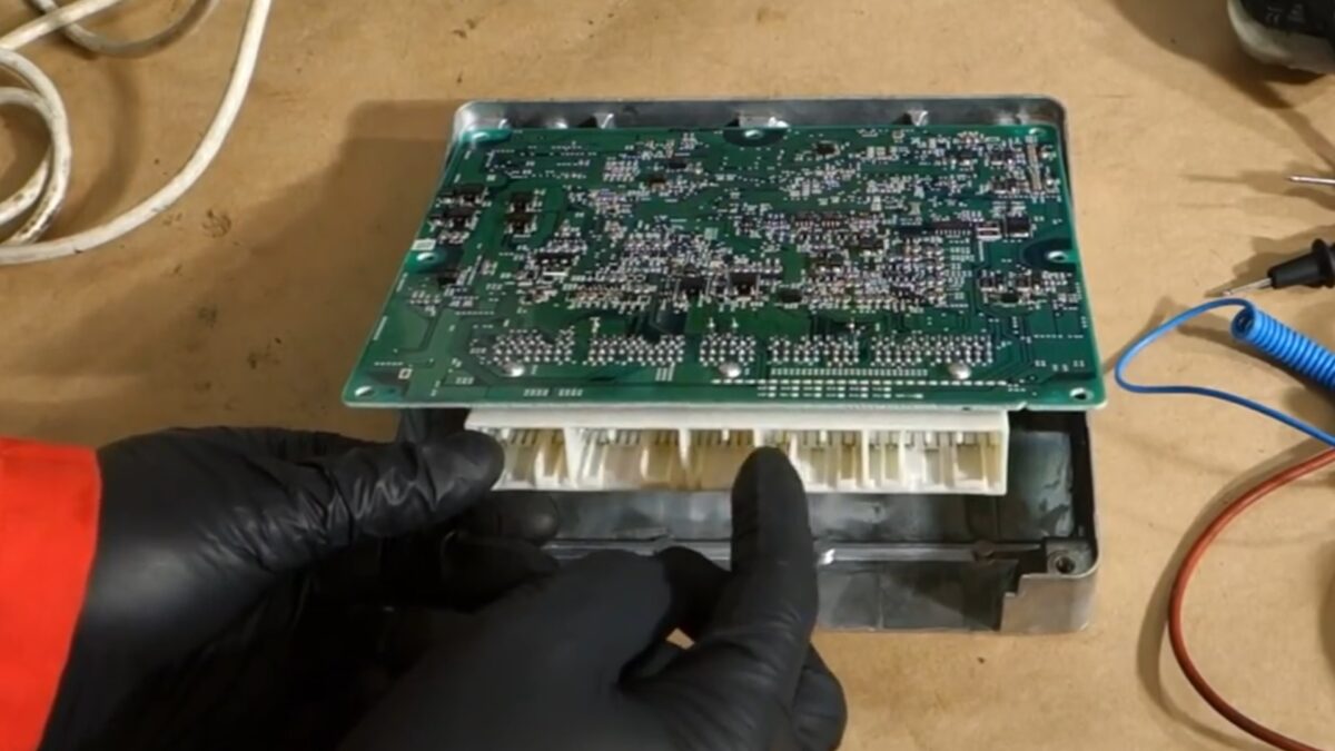
Once all technical documents are restored, the principle extends to redevelopment and redesign for real production. The recovered Gerber file, schematic diagram, layout drawing, bom list, and netlist are converted into manufacturing-ready CAD data. Engineers must pay close attention to impedance control, grounding strategies, EMC/EMI performance, and thermal design—critical factors for ECU reliability in harsh bulldozer environments. In some cases, redesign or redevelopment is required to replace obsolete components, optimize the layout, or improve production yield, while still maintaining functional equivalence with the original ECU board. This stage bridges reverse engineering and practical mass production.
Buldozer Motor Kontrol Ünitesinde (ECU) kullanılan bir PCB’nin tersine mühendisliği, motor hızını, tork çıkışını ve yakıt enjeksiyon kontrolünü izleyen orijinal elektronik tasarımı kurtarmayı, geri yüklemeyi ve tam olarak anlamayı amaçlayan sistematik bir teknik süreçtir. İlke, katman yapısı, malzemeler ve sinyal bütünlüğü kısıtlamaları da dahil olmak üzere fiziksel kartın eksiksiz bir analiziyle başlar. Profesyonel tersine mühendislik yöntemleri sayesinde mühendisler, orijinal ECU PCB’sinden Gerber dosya verilerini çıkarabilir, yerleşim çizimini yeniden oluşturabilir ve güç yönetimi, sensör arayüzleri ve mikrodenetleyici üniteleri gibi temel fonksiyonel blokları tanımlayabilirler. Bu temel adım, ağır hizmet buldozer operasyonu için gerekli olan orijinal elektriksel performansı ve çevresel dayanıklılığı korurken doğru kopyalama, klonlama veya çoğaltma işlemlerini mümkün kılar. ECU tersine mühendisliğinin temel bir aşaması, fiziksel kartı dijital tasarım dokümantasyonuna dönüştürmeyi içerir. Şematik diyagramı ve netlisti hassas bir şekilde yeniden oluşturmak için yüksek çözünürlüklü tarama, katman katman ayırma ve ağ izleme yöntemleri uygulanır. Bu aşamada mühendisler, motor hızı algılama, tork hesaplama ve yakıt enjeksiyon zamanlamasıyla ilgili her sinyal yolunu yeniden üretirler. Ardından, otomotiv sınıfı entegre devreler ve koruma cihazları da dahil olmak üzere tüm aktif ve pasif bileşenler tanımlanarak doğrulanmış bir malzeme listesi oluşturulur. Bu kapsamlı yeniden yapılandırma süreci, orijinal ECU kartının aslına sadık kalınarak yeniden üretilmesine veya onarılmasına olanak tanıyarak, orijinal üreticilerin artık destek sağlamadığı durumlarda yenileme, yedek parça üretimi veya uzun vadeli yedek parça tedariği gibi görevleri destekler.
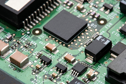
Despite its value, ECU PC board reverse engineering presents notable difficulties. Multilayer structures, encrypted microcontrollers, proprietary fuel injection algorithms, and strict automotive reliability standards increase technical complexity. Errors in copying sensor interfaces or timing-critical circuits can impact engine torque control and fuel efficiency. However, when executed correctly, reverse engineering allows manufacturers and service providers to recreate, reproduce, refurbish, or redesign ECU boards with high confidence. This technology is widely used for maintenance, system upgrades, localization of production, and lifecycle extension of bulldozer engine control systems, delivering both economic and operational benefits.