

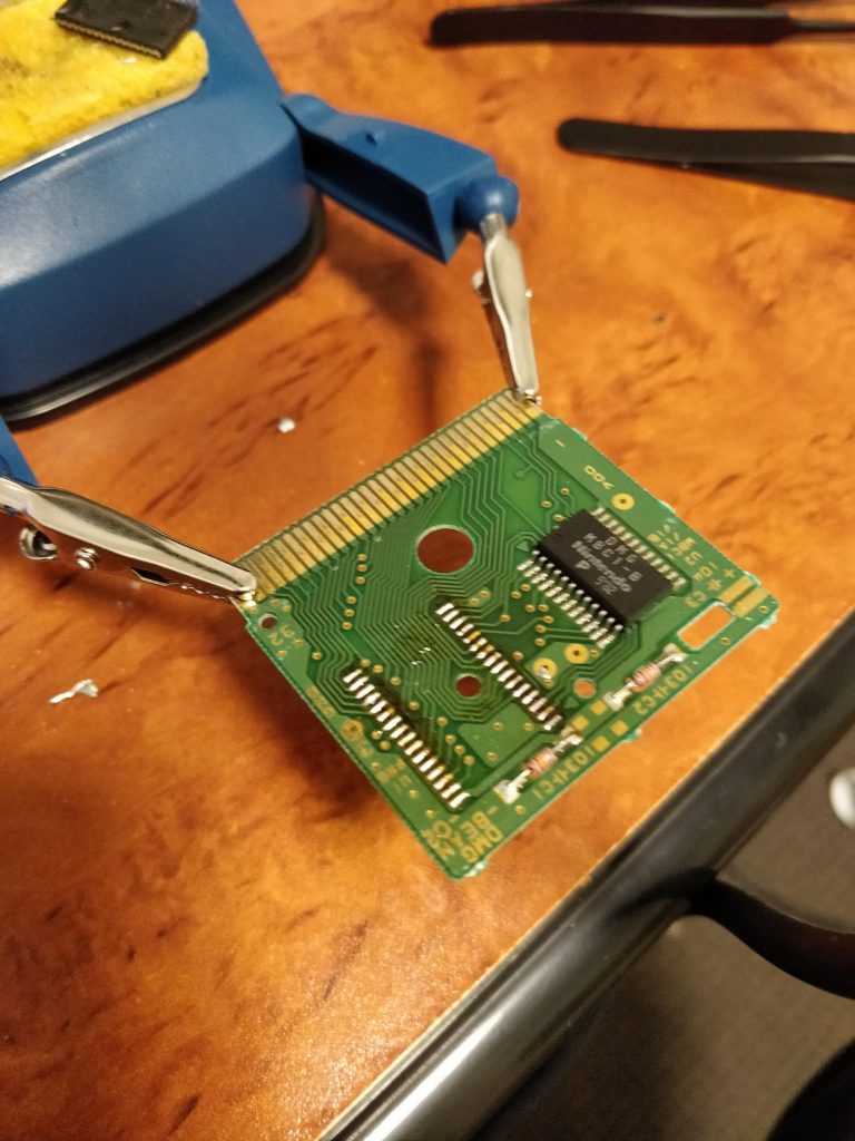
PC Board Reverse Engineering Introduction
Each PC Board Reverse Engineering consists of several, mostly independent, objects. This chapter gives an overview of the object types and their relationship to each other. For a complete description of how to assure the quality of Printed wiring Board Reverse Engineering. The layout is generated on-screen on a grid that can have its origin at any desired location. The X coordinate increases to the right, Y increases down to the bottom. All distances and sizes in Pcb are measured in mils (0.001 inch). One unit on the coordinate display is one mil in distance on the board.
The grid may be set on a metric pitch, but is only correct to within the nearest +/- 0.01 mil because Pcb stores all dimensions as integer multiples of 1/100 of a mil or 0.00001 inch. The sections in this chapter are sorted by the order of appearance of the objects within a layout file from PCB reverse engineering.
2.1 Symbols
The top object is the Printed wiring Board copying itself. It uses a set of symbols that resides at the first logical level. Each symbol is uniquely identified by a seven bit ASCII code. All layout objects share the same set of symbols. These symbols are used to form text objects on the silkscreen and copper layers. Undefined symbols are drawn as filled rectangles. Every font file is preprocessed by a user-defined command when it is loaded. For details see ‘fontCommand”.
2.2 Vias
Vias provide through-hole connectivity across all layers. While vias look a lot like element pins, don’t use vias for adding elements to the layout from circuit board Reverse Engineering quality control, even if that seems easier than creating a new element. The default solder-mask will cover over vias, so you won’t be able to solder to them. Of course, you can change this so that vias also have solder-mask cut-outs, but it is not the default. Vias are also useful for defining arbitrary drill points such as those used for mounting a board. Vias used in this way have a special flag set so that they have no annular copper ring, and also appear in the unplated drill file. Ctrl-H key over a via switches it between being a pure-mounting hole and a regular via. You can assign a name to a via, which is useful during the creation of new element definitions. Each via exists on all copper layers. (i.e. blind and buried vias are not supported)
Tags: pcb board reverse engineering,pcb card reverse engineering,pcb circuit board reverse engineering,pcb reverse engineering,pcba reverse engineering,Printed Circuit Board Reverse Engineering,printed wiring board reverse engineering,pwb reverse engineering,pwba reverse engineering