"Everything we build starts with design engineering. CECL manufactured boards for one of our products. It went perfectly – a real success.It is really an high quality service they have provided to us!"
By Nile Smith from Sinotech Inc.
“We had several very old device with obsolete boards need to be replaced –through CECL professional service.We got what we needed, and we’ve been using the results of the work without any problem till now.”
By Richard Anderson from TWP system Inc.
"Guys from CECL manufacture PCBs we use in one of our products, a clinometer and we’ve never had a problem with anything. The boards come in, they work. And, their team is very responsive."
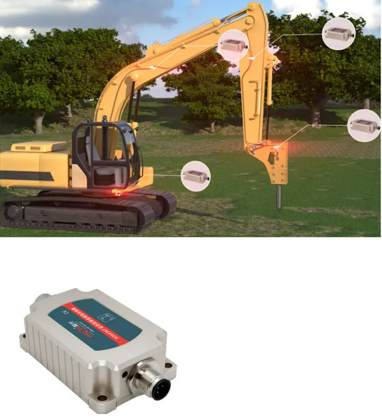
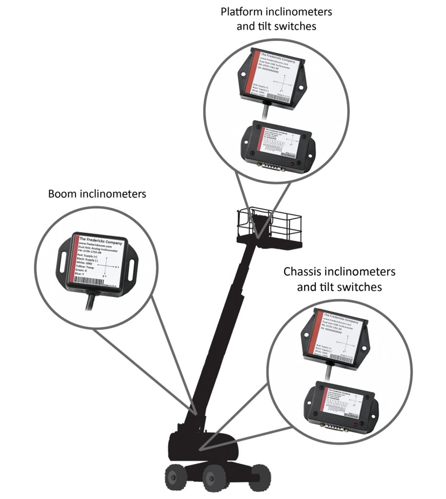
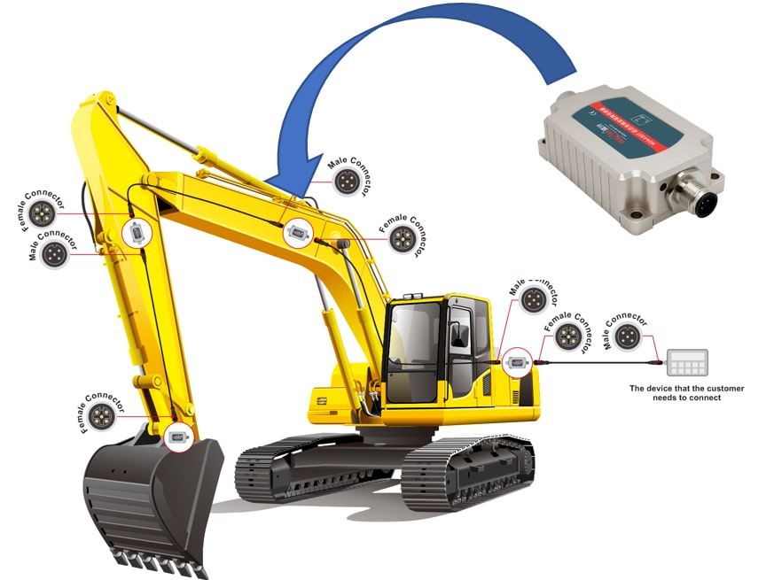
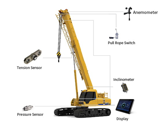
Optimize Sensor Interface Printed Circuit Board Reverse Engineering is a highly practical engineering approach for restoring and enhancing sensor interface boards used in excavators. These boards serve as the critical link between pressure, tilt, temperature, and proximity sensors and the main control system. When original design files are lost, components become obsolete, or performance no longer meets operational demands, PCB reverse engineering allows companies to recover functionality and selectively optimize the design for long-term use.
Il processo inizia con un’analisi fisica ed elettrica dettagliata della scheda esistente. Gli ingegneri ispezionano attentamente il PCB nudo per recuperare la topologia del circuito, i percorsi dei segnali e la distribuzione dell’alimentazione. Tracciando le connessioni e identificando i componenti, è possibile ripristinare progressivamente lo schema elettrico originale, chiarendo come i segnali dei sensori analogici vengono condizionati, filtrati, amplificati e convertiti per l’elaborazione digitale. Questa fase è essenziale per comprendere la sensibilità al rumore, la precisione dei sensori e la stabilità dell’interfaccia. Successivamente, viene ricreata la struttura fisica della scheda. L’impedenza dei layer, la strategia di messa a terra e il posizionamento dei componenti vengono documentati per generare un disegno di layout accurato, un file Gerber e output di netlist. Questi documenti consentono agli ingegneri di copiare, clonare o replicare il PCB dell’interfaccia del sensore in tutta sicurezza. Durante questa fase, spesso si presentano opportunità per riprogettare i punti deboli, come il miglioramento del disaccoppiamento, la separazione delle masse analogiche e digitali o il miglioramento della robustezza EMC senza modificare le funzionalità principali. Una volta completata la documentazione, il progetto passa alla produzione. Il PCB viene rifabbricato utilizzando i dati Gerber recuperati, garantendo la coerenza nei materiali e nello spessore della scheda. L’approvvigionamento dei componenti viene effettuato rigorosamente in base alla distinta base verificata. Per sensori, amplificatori operazionali, convertitori A/D o dispositivi di protezione non più disponibili, gli ingegneri possono rinnovare il progetto selezionando componenti equivalenti ed eseguendo una riprogettazione controllata di circuiti specifici.
The process begins with a detailed physical and electrical analysis of the existing board. Engineers carefully inspect the bare PCB to recover circuit topology, signal paths, and power distribution. By tracing connections and identifying components, the original schematic diagram can be progressively restored, clarifying how analog sensor signals are conditioned, filtered, amplified, and converted for digital processing. This stage is essential for understanding noise sensitivity, sensor accuracy, and interface stability.
As we all know, PCB reverse engineering is a process to restore circuit board documents, Optimize Printed Circuit Board Reverse Engineering will help to greatly improve the efficiency and preciseness of schematic, gerber file and PCB board layout design;
As we all know, PCB reverse engineering is a process to restore circuit board documents, Optimize Printed Circuit Board Reverse Engineering will help to greatly improve the efficiency and preciseness of schematic, gerber file and PCB board layout design
1 Shorten the connection distance among the high frequency component on the Printed Circuit Board to decrease the EMI interference;
2 the weight over 20g components when reverse engineering Printed Circuit Board should be fixed on a socket instead of assembly on the printed circuit board directly when reverse engineering it;
3 the component with high heat dissipation issue must be considered to prevent the defects and rework and all the thermo-sensitive part must keep away from heat source when printed circuit board reverse engineering;
Le processus débute par une analyse physique et électrique détaillée de la carte existante. Les ingénieurs examinent minutieusement le circuit imprimé nu afin de reconstituer la topologie du circuit, les chemins des signaux et la distribution de l’alimentation. En traçant les connexions et en identifiant les composants, le schéma original peut être progressivement reconstitué, ce qui permet de comprendre comment les signaux analogiques des capteurs sont conditionnés, filtrés, amplifiés et convertis pour le traitement numérique. Cette étape est essentielle pour appréhender la sensibilité au bruit, la précision du capteur et la stabilité de l’interface. Ensuite, la structure physique de la carte est recréée. L’empilement des couches, l’impédance des pistes, la stratégie de mise à la terre et le placement des composants sont documentés afin de générer un schéma d’implantation précis, un fichier Gerber et une netlist. Ces documents permettent aux ingénieurs de copier, cloner ou reproduire le circuit imprimé d’interface du capteur en toute confiance. Durant cette phase, des opportunités se présentent souvent pour corriger les points faibles, comme l’amélioration du découplage, la séparation des masses analogiques et numériques ou le renforcement de la robustesse CEM sans altérer les fonctionnalités principales. Une fois la documentation terminée, le projet passe à la fabrication. Le circuit imprimé est refabriqué à partir des données Gerber reconstituées, garantissant ainsi la constance des matériaux et de l’épaisseur de la carte. L’approvisionnement en composants est effectué en stricte conformité avec la nomenclature validée. Pour les capteurs, amplificateurs opérationnels, convertisseurs analogique-numérique ou dispositifs de protection devenus obsolètes, les ingénieurs peuvent moderniser la conception en sélectionnant des composants équivalents et en procédant à un redéveloppement contrôlé des circuits concernés.
4 all the arrangement of component must be parallel which will have better cosmetic and easier to solder for mass production, Printed Circuit Board reverse engineering should be 4:3 ratio. And the width of track shouldn’t alter suddenly to avoid the inconsistency;
5 Printed Circuit Board can probably swelled and copper foil strip off the printed wiring board due to constant heating. So when reverse engineering printed wiring board we should avoid the application of large size of copper foil;
Next, the physical structure of the board is recreated. Layer stack-up, trace impedance, grounding strategy, and component placement are documented to generate accurate layout drawing, Gerber file, and netlist outputs. These documents allow engineers to copy, clone, or replicate the sensor interface PCB with confidence. During this phase, opportunities often arise to redesign weak points, such as improving decoupling, separating analog and digital grounds, or enhancing EMC robustness without changing core functionality.
Once documentation is complete, the project transitions to manufacturing. The PCB is remanufactured using the recovered Gerber data, ensuring consistency in materials and board thickness. Component procurement is carried out strictly according to the verified BOM list. For sensors, op-amps, ADCs, or protection devices that are no longer available, engineers may refurbish the design by selecting equivalent parts and performing controlled redevelopment of specific circuits.
Der Prozess beginnt mit einer detaillierten physikalischen und elektrischen Analyse der vorhandenen Leiterplatte. Ingenieure untersuchen die unbestückte Leiterplatte sorgfältig, um die Schaltungstopologie, Signalwege und die Stromverteilung zu ermitteln. Durch das Nachverfolgen von Verbindungen und die Identifizierung von Bauteilen kann der ursprüngliche Schaltplan schrittweise wiederhergestellt werden. Dadurch wird deutlich, wie analoge Sensorsignale aufbereitet, gefiltert, verstärkt und für die digitale Verarbeitung umgewandelt werden. Diese Phase ist entscheidend für das Verständnis der Rauschempfindlichkeit, der Sensorgenauigkeit und der Stabilität der Schnittstelle. Anschließend wird die physikalische Struktur der Leiterplatte nachgebildet. Lagenaufbau, Leiterbahnimpedanz, Erdungsstrategie und Bauteilplatzierung werden dokumentiert, um präzise Layoutzeichnungen, Gerber-Dateien und Netzlisten zu erstellen. Mithilfe dieser Dokumente können Ingenieure die Leiterplatte der Sensorschnittstelle zuverlässig kopieren, klonen oder replizieren. In dieser Phase ergeben sich häufig Möglichkeiten, Schwachstellen zu beheben, z. B. durch Verbesserung der Entkopplung, Trennung von analoger und digitaler Masse oder Erhöhung der EMV-Robustheit, ohne die Kernfunktionalität zu beeinträchtigen. Nach Abschluss der Dokumentation geht das Projekt in die Fertigung über. Die Leiterplatte wird anhand der ermittelten Gerber-Daten neu gefertigt, um die Konsistenz von Materialien und Leiterplattendicke zu gewährleisten. Die Komponentenbeschaffung erfolgt strikt gemäß der verifizierten Stückliste. Sollten Sensoren, Operationsverstärker, AD-Wandler oder Schutzbausteine nicht mehr verfügbar sein, können die Ingenieure das Design durch die Auswahl äquivalenter Bauteile und eine kontrollierte Neuentwicklung bestimmter Schaltungen modernisieren.
Assembly follows standard PCBA processes, after which functional testing is performed. Pressure, tilt, temperature, and proximity inputs are simulated to validate signal accuracy and response time. Only after successful verification can the design be reproduced or duplicated for deployment in excavator systems.
Converting reverse-engineered documents into real production requires attention to manufacturing tolerances, calibration requirements, and environmental durability. The primary usage of this technique is extending equipment life, reducing downtime, and enabling localized supply of spare boards. However, difficulties may include multilayer complexity, mixed-signal interference, and limited access to original firmware behavior.
El proceso comienza con un análisis físico y eléctrico detallado de la placa existente. Los ingenieros inspeccionan cuidadosamente la PCB sin procesar para recuperar la topología del circuito, las rutas de señal y la distribución de energía. Al rastrear las conexiones e identificar los componentes, se puede restaurar progresivamente el diagrama esquemático original, lo que aclara cómo se acondicionan, filtran, amplifican y convierten las señales analógicas de los sensores para su procesamiento digital. Esta etapa es esencial para comprender la sensibilidad al ruido, la precisión del sensor y la estabilidad de la interfaz. A continuación, se recrea la estructura física de la placa. Se documentan el apilado de capas, la impedancia de las trazas, la estrategia de conexión a tierra y la ubicación de los componentes para generar planos de diseño, archivos Gerber y salidas de lista de conexiones precisos. Estos documentos permiten a los ingenieros copiar, clonar o replicar la PCB de la interfaz del sensor con confianza. Durante esta fase, a menudo surgen oportunidades para rediseñar los puntos débiles, como mejorar el desacoplamiento, separar las conexiones a tierra analógicas y digitales o aumentar la robustez de la compatibilidad electromagnética (EMC) sin modificar la funcionalidad principal. Una vez completada la documentación, el proyecto pasa a la fase de fabricación. La PCB se remanufactura utilizando los datos Gerber recuperados, lo que garantiza la consistencia de los materiales y el grosor de la placa. La adquisición de componentes se realiza estrictamente de acuerdo con la lista de materiales verificada. En el caso de sensores, amplificadores operacionales, convertidores analógico-digitales (ADC) o dispositivos de protección que ya no están disponibles, los ingenieros pueden renovar el diseño seleccionando piezas equivalentes y realizando un rediseño controlado de circuitos específicos.
When executed correctly, Optimize Sensor Interface Printed Circuit Board Reverse Engineering delivers reliable, production-ready documentation and hardware, enabling stable sensor integration and improved performance in demanding construction environments.
Circuit Engineering Company Limited continues to be recognized as the Southern China Leader in Services for PCB Reverse Engineering, PCB card cloning, PCB Copy and replicate printed circuit board. With the advancement of today’s modern circuit board technology, it is more important than ever to have specialists available to help you at a moment’s notice. Our engineering and commercial teams collectively have a vast amount of electronic experience covering field include Consumer Electronics, Industrial Automation Electronics, Wireless Communication Electronics., etc. Circuit Engineering Company Limited have gained an excellent reputation for the reliability and speed of service with many large manufacturing organisations, throughout a diverse range of industries. We are excited about the opportunity to serve you, and assure you that we will continue to advance our knowledge, hone our skills and maintain the state-of-the-art equipment needed to provide you with the highest level of service possible. Our mission is simple. Save you money, save you time, and make your company more profitable. For more information please Contact Us through email or by phone.