Multi-layer PCB Board Lamination Rules
With the improvement of Multi-layer PCB Board Lamination Rules and the increase in consumer demand for faster and more powerful products, PCB has changed from a basic two-layer board to multi-layer PCB board with 4, 6, and up to 10 to 30 layers of dielectric and conductors.

Why increase the number of layers? Having more layers can increase the power distribution of the circuit board, reduce cross-talk, eliminate electromagnetic interference and support high-speed signals.
The number of layers used for the PCB depends on the application, operating frequency, pin density and signal layer requirements by stacking two layers, the top layer (ie, layer 1) is used as a signal layer.
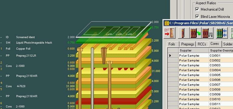
The four-layer stack uses the top and bottom layers (or the 1st and 4th layers) as the signal layer. In this configuration, the 2nd and 3rd layers are used as planes. The pre-preg layer bonds two or more double-sided panels together and acts as a dielectric between the layers.

The 6-layer PCB adds two copper layers, and the second and fifth layers serve as planes. Layers 1, 3, 4, and 6 carry signals. Proceed to the six-layer structure, the inner layer two, three (when it is a double-sided board) and the fourth five (when it is a double-sided board) as the core layer, and the prepreg (PP) is sandwiched between the core boards.

