PCB Reverse Engineering, PCB Clone & PCB Copy Services

Printed Circuit Board Reverse Engineering Material Analysis

In the fast-evolving world of electronics, older devices are often retired not because they fail, but because their design documentation is lost, and replacements are no longer available. For companies relying on specialized or discontinued products, this can be a major obstacle. The solution? Printed Circuit Board Reverse Engineering Material Analysis—a highly specialized service that allows engineers to recover, restore, or recreate crucial technical data by analyzing the very materials and structure of the original PCB.

Analisi dei materiali per il reverse engineering di circuiti stampati: un servizio altamente specializzato che consente agli ingegneri di recuperare, ripristinare o ricreare dati tecnici cruciali analizzando i materiali e la struttura del PCB originale. Questa forma avanzata di reverse engineering va oltre la semplice estrazione di diagrammi schematici, file Gerber, distinte base o disegni di layout. Comporta una valutazione completa del substrato del PCB, delle tracce di rame, degli strati dielettrici, della maschera di saldatura e persino delle strutture dei fori, consentendo una duplicazione o una riprogettazione accurata del prodotto originale.

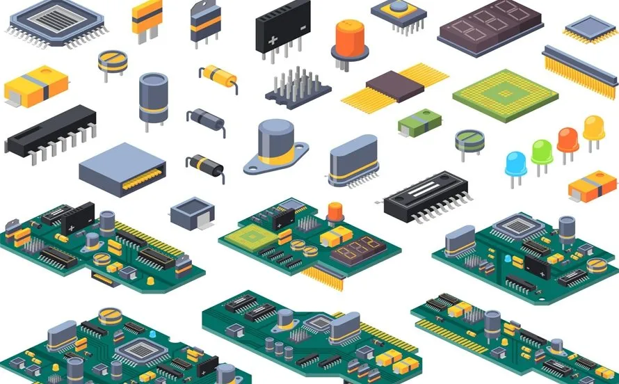
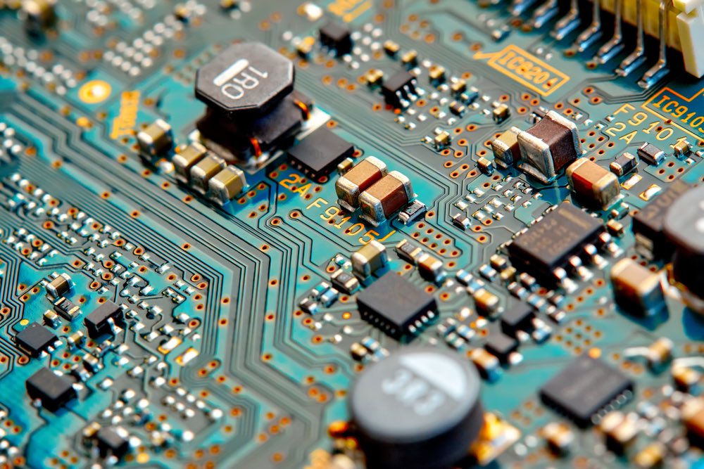
This advanced form of reverse engineering dives deeper than just extracting schematic diagrams, Gerber files, BOM lists, or layout drawings. It involves a comprehensive assessment of the PCB’s substrate, copper traces, dielectric layers, solder mask, and even via structures, which allows accurate duplication or redesign of the original product.


Why Material Analysis Matters in PCB Cloning

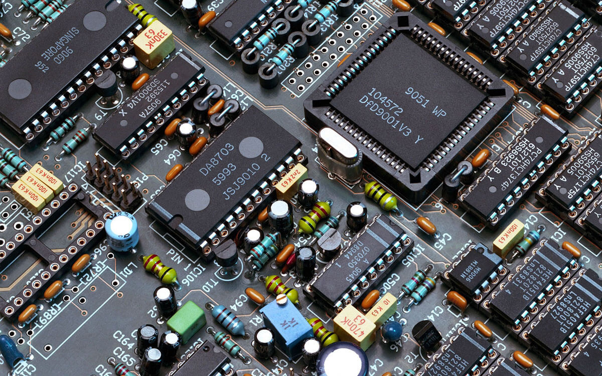
In conventional PCB reverse engineering, the focus is often on mapping out circuit paths and identifying components. However, this only tells half the story. A truly accurate reproduction also depends on understanding what the board is made of and how the materials affect electrical performance, thermal stability, and mechanical endurance.

For example, high-frequency RF PCBs used in radar systems, military communication gear, or medical imaging equipment require very specific substrates such as FR-4, Rogers, or ceramic-based materials. If these properties are not properly replicated, the final product may perform poorly or fail in real-world conditions.

Анализ материалов для обратного проектирования печатных плат — узкоспециализированная услуга, позволяющая инженерам восстановить, восстановить или воссоздать критически важные технические данные, анализируя материалы и структуру исходной печатной платы. Эта продвинутая форма обратного проектирования выходит за рамки простого извлечения принципиальных схем, файлов Gerber, спецификаций материалов или чертежей топологии. Она включает в себя комплексную оценку подложки печатной платы, медных дорожек, диэлектрических слоёв, паяльной маски и даже структуры переходных отверстий, что позволяет точно скопировать или перепроектировать исходное изделие.

This is where Printed Circuit Board Reverse Engineering Material Analysis plays a critical role. Techniques like cross-section microscopy, FTIR spectroscopy, scanning electron microscopy (SEM), and X-ray fluorescence (XRF) are used to evaluate:

  • PCB layer count and thickness
  • Copper weight and plating type
  • Dielectric constant of insulation layers
  • Thermal conductivity and flame resistance
  • Solder mask and silkscreen material properties

With this level of analysis, the remanufactured or redesigned PCB board can closely match or even exceed the performance of the original.


Practical Applications Across Critical Industries

Material analysis in PCB reverse engineering is especially valuable for industries that rely on high-performance, long-lifecycle electronics. This includes:

  • Aerospace & Defense: Flight control systems, avionics, UAV and missile boards
  • Medical Devices: Diagnostic equipment, MRI and CT scan controller boards
  • Industrial Automation: PLC boards, robotic control systems, sensor interfaces
  • Telecommunications: Satellite modem PCBs, repeater systems, 5G network cards
  • Energy Sector: Power inverters, battery management PCBs, grid interface systems

In many of these cases, the original supplier may no longer exist, and documentation such as netlists, schematics, or Gerber data may be unavailable. Our service enables businesses to restore and replicate these critical PCBs through accurate material-based reverse engineering, ensuring operational continuity and compliance.

Reverse Engineering von Leiterplatten – ein hochspezialisierter Service, der es Ingenieuren ermöglicht, wichtige technische Daten durch Analyse der Materialien und der Struktur der Originalplatine wiederherzustellen oder neu zu erstellen. Diese fortschrittliche Form des Reverse Engineering geht tiefer als nur das Extrahieren von Schaltplänen, Gerber-Dateien, Stücklisten oder Layoutzeichnungen. Sie umfasst eine umfassende Bewertung des Leiterplattensubstrats, der Kupferleiterbahnen, der dielektrischen Schichten, der Lötstoppmaske und sogar der Via-Strukturen, wodurch eine präzise Duplizierung oder Neugestaltung des Originalprodukts ermöglicht wird.

Strategic Value to Businesses and OEMs

Whether you are a systems integrator, defense contractor, or medical equipment provider, the ability to recreate a legacy board through material analysis opens doors to refurbishment, redevelopment, and even product redesign. This minimizes downtime, cuts replacement costs, and preserves your technological investment.

More than just a technical solution, Printed Circuit Board Reverse Engineering Material Analysis is a powerful strategy for any business facing obsolescence. With it, we don’t just bring back a board—we bring back the future of your product. Improper cutting of the sample could affect the hardness readings or the interpretation of the heat treating process.

प्रिंटेड सर्किट बोर्ड रिवर्स इंजीनियरिंग मटेरियल एनालिसिस—एक अत्यधिक विशिष्ट सेवा है जो इंजीनियरों को मूल पीसीबी की सामग्री और संरचना का विश्लेषण करके महत्वपूर्ण तकनीकी डेटा को पुनर्प्राप्त, पुनर्स्थापित या पुनः निर्मित करने की अनुमति देती है। रिवर्स इंजीनियरिंग का यह उन्नत रूप केवल योजनाबद्ध आरेखों, गेरबर फ़ाइलों, बीओएम सूचियों या लेआउट रेखाचित्रों को निकालने से कहीं अधिक गहन है। इसमें पीसीबी के सब्सट्रेट, तांबे के अंशों, परावैद्युत परतों, सोल्डर मास्क और यहाँ तक कि संरचनाओं का व्यापक मूल्यांकन शामिल है, जिससे मूल उत्पाद का सटीक प्रतिरूपण या पुनः डिज़ाइन संभव हो पाता है।