

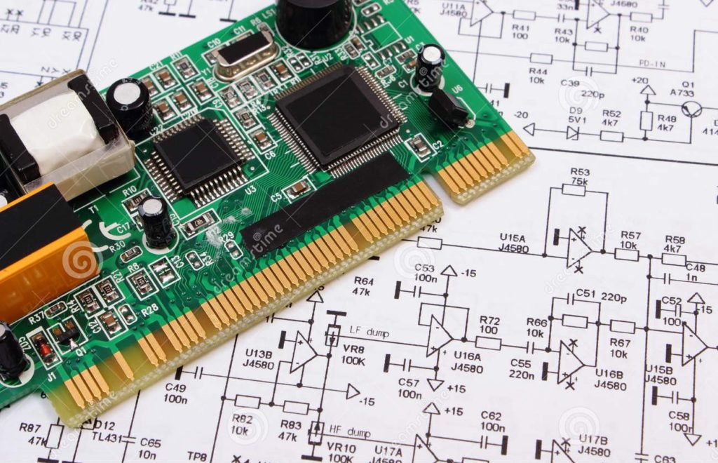
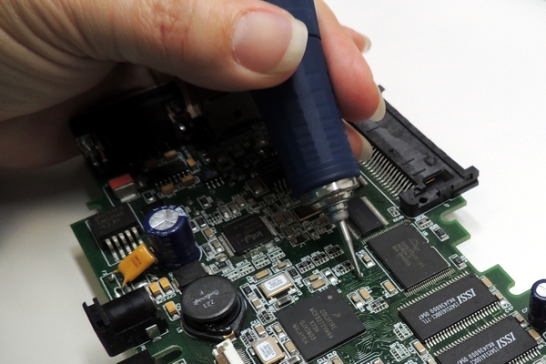
High Speed Printed Wiring Board Reverse Engineering
High speed Printed Wiring Board reverse engineering to great extent is subject to a restricted method. Nowadays, design engineer input the electronic design data and other design restricted terms into the PWB Board cloning software for high speed design and layout, but the signal integrity issue and other complexity problems accumulated make it become more difficult.
So it is necessary to have the design simulated and comprehesion which give rise to the requirement of new design environment. From the eletrical features to the Printed Wiring Board manufacture skill, design engineers must install the restricted terms.
In a ideal reverse engineering PCB board background platform, they can reverse engineering pwb not only depends on the conductor length, electro-magnetic interference and cross-talk, but also regarding distance among components, height restriction and rotating angle installation among the components.
In order to swiftly generate these rules, the PCB Board schematic design must have strong topology analysis and all of the possible situations. And it is best to have design engineers to use signal integrity analysis engine and make change in the topology and research other terminal solutions, also make its interacting functionality with each other over the delay terms, circuit layer option and other conductors distance, which makes the effect on the signal integrity to the minimum level. This functions can also combine with other components placement and other functions. As a result of that, design engineer can define the primitive component installation and understand the Printed Wiring Board strategy features. All in one, new design environment must provide a strong restricted term management capability to facilitate the designer organizations and other publich informations.
Tags: pcb assemble reverse engineering,pcb board reverse engineering,pcb card reverse engineering,pcb reverse engineering,pcba reverse engineering,Printed Circuit Board Reverse Engineering,printed wiring board reverse engineering,pwb reverse engineering,pwba reverse engineering