

High Resolution Printer PCBA Cloning
High Resolution Printer PCBA Cloning refers to restoring the schematic diagram, layout and gerber file from printed circuit board, the PCBA electronic card drawing can be redesigned to suit for the new requirement from end user;
After you get started of your High Resolution Printer PCBA Cloning project with us, all the necessary files will be submited in below format through which your High Resolution Printer PCBA can be manufacture and assembly anywhere in the world, we can ensure the accuracy of your data by means of prototype running.
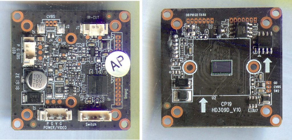
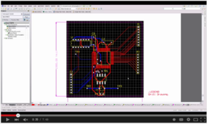
Here is sample of files and drawings you will receive, based on a typical double layer High Resolution Printed circuit board reverse engineering with components mounted on two sides:
Bottom Side of Gerber File from High Resolution Printer PCB board:
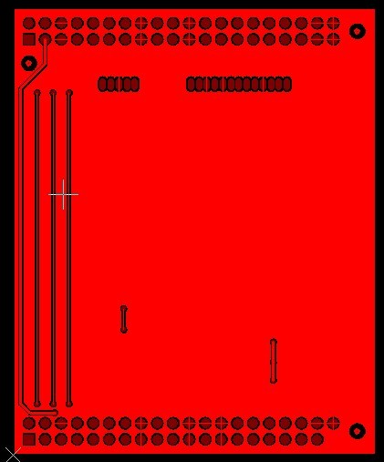
Top Side of Gerber File from High Resolution Printer PCB card:

Circuit Engineering Company Limited provide a complete PCB Reverse Engineering, PCB Clone and PCB Restoration service, Rapid Prototyping and functional test services using the latest technologies combined with traditional skills for a wide range of industries. By integrating our traditional skills with the latest technologies, we can offer clients a comprehensive portfolio of product development services all under one roof. For more details please contact our customer
service team.
Tags: double side pcba cloning,flexible pcba cloning,multilayer pcba cloning,rigid flex pcba cloning,single side pcba cloning,клон pcb bom,клон pcb component list,клон pcb design,клон pcb gerber file,клон pcb layout,клон pcb schematic