

Electronic Printed Circuit Board Introduction
Electronic printed circuit board are by far the most common method of assembling modern electronic circuits. Comprised of a sandwich of one or more insulating layers and one or more copper layers which contain the signal traces and the powers and grounds, the design of the layout diagram of Printed circuit board can be as demanding as the design of the electrical circuit.
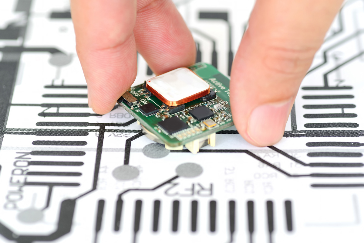
Most modern systems consist of multi-layer PCB boards of anywhere up to eight layers (or sometimes even more). Traditionally, components were mounted on the top layer in holes which extended through all layers. These are referred as through hole components.
Use Schematic design tool to draw it then generate corresponded net-list, of course in the special circumstance such as a simple PCB board, there is no need to carry out the schematic drawing designing if the net-list has existed, enter directly into the PCB design system, in the system can pick up the component footprint directly to generate net-list manually.
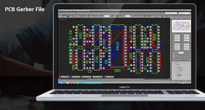
Change the netlist manually, define the fixed pin on the components which has been designed on the soldering pad of schematic diagram, for those pins without any physical connection can lead to the ground or protection ground, etc. categorize the pins with different names with schematic and PCB footprint align with the PCB library especially the diode, transistor, etc