

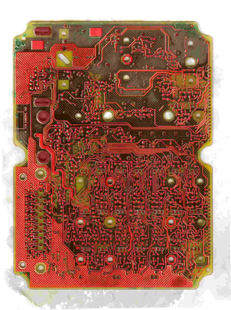
Electronic PCB Card Reverse Engineering Text
Electronic PCB Card Reverse Engineering Text is a part of job when recreate the fonts, labels and designators from original printed circuit board, Text objects should be used to label a PCB board layout design or to put additional information on the circuit board. Elements have their ‘layout-name’ labels on the silk-screen layer. If you are making a board without a silkscreen, you can use copper text to label the elements, but you have to do this manually.
Text is always horizontal when first created, but the rotate mode can align it along 0, 90, 180 and 270 degree angles. Text on the far side of the board will automatically appear mirror-imaged.
Warning: TEXT OBJECTS ON A COPPER LAYER CREATE COPPER LINES BUT THEY ARE NOT SCANNED FOR CONNECTIONS OR TESTED FOR CREATING SHORTS VS. THE NETLIST. NEITHER ARE TEXT OBJECTS TESTED AGAINST ANY DESIGN RULES.
Reverse Engineering pcb circuit board Nets
Layout files from Electronic pcb board restoration also contain the netlist that describes how the elements are supposed to be interconnected. This list of connections can be loaded from a netlist file, or entered by drawing rat-lines as described previously. Each net has a name and routing style associated with it. The net contains a list of all element layout-name names and pin numbers that should be connected to the net. Loading a netlist file will replace all existing nets with the ones from the file. The Netlist window provides an easy way to browse through the net list. You can display the rat’s-nest by selecting ‘optimize rats-nest’ from the Connects menu. If you move or rotate elements, the rat’s-nest will automatically follow the movements, but they won’t necessarily show the shortest paths until you optimize them again.
Tags: reverse engineering pcb card artwork,reverse engineering pcb card bom,reverse engineering pcb card component list,reverse engineering pcb card design,reverse engineering pcb card diagram,reverse engineering pcb card drawing,reverse engineering pcb card gerber file,reverse engineering pcb card layout,reverse engineering pcb card part list,reverse engineering pcb card schematic