eGaN FETs Layout in PCB Duplication
eGaN FETs Layout in PCB Duplication
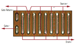
eGaN FETs Layout in PCB Duplication are available in a Wafer Level Chip-Scale Package (WLCSP) with terminals in a Land Grid Array (LGA) format. Some of these devices do not offer a separate gate-return source pin, but rather a number of very low inductance LGA solder bars as shown in below figure.
These parts can be treated in the same way as one provided with a dedicated gate return pin or bar, by allocating the source pads closest to the gate to act as the “star” connection point for both the gate loop and power loop. The layout of the gate and power loops are then separated by having the currents flow in opposite or orthogonal directions as shown in above figure.
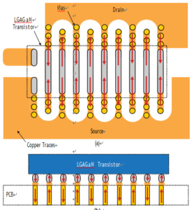
By interleaving the drain and source terminals on one side of the device, a number of small loops with opposing currents are generated that will decrease the overall inductance through magnetic field self-cancellation. This is not only true for the PCB traces shown in below figure,
but also for the vertical LGA solder bars and the interlayer connection vias shown in above figure. With multiple small magnetic field cancelling loops formed, the total magnetic energy, and therefore inductance, is significantly reduced.

eGaN FETs Layout in PCB Duplication
A further reduction in partial loop inductance is possible by bringing both drain and source currents out on both sides of the device from the centerline and duplicating the magnetic field cancellation effect. This works by reducing the current in each conductor, thus further reducing the energy stored, and the shorter current path yields a lower inductance.


