

MINI-DIP SOIC op amp PCB guard layouts
Modern assembly practices have favored smaller plastic packages such as eight pin MINI-DIP SOIC op amp PCB guard layouts. Some suggested partial layouts for guard circuits using these packages are shown in the next two figures. While guard traces may also be possible with even more tiny op amp footprints, such as SOT-23 etc., the required trace separations become even more confining, challenging the layout designer as well as the manufacturing processes.
MINI-DIP SOIC op amp PCB guard layouts
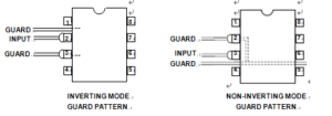
For the ADI “N” style MINI-DIP package, below Figure illustrates how guarding can be accomplished for inverting (left) and noninverting (right) operating modes. This setup would also be applicable to other op amp devices where relatively high voltages occur at pin 1 or 4. Using a standard eight pin DIP outline, it can be noted that this package’s 0.1″ pin spacing allows a PC trace (here, the guard trace) to pass between adjacent pins.
This is the key to implementing effective DIP package guarding, as it can adequately prevent a leakage path from the –VS supply at pin 4, or from similar high potentials at pin 1.
PCB Guard Patterns for Inverting and Noninverting Mode Op
Amps Using Eight Pin MINI-DIP (N) Package
For the left-side inverting mode, note that the Pin 3 connected and grounded guard traces surround the op amp inverting input (Pin 2), and run parallel to the input trace. This guard would be continued out to and around the source and feedback connections of Figure 12-36 (or other similar circuit), including an input pad in the case of a cable.
In the right-side noninverting mode, the guard voltage is the feedback divider voltage to Pin 2. This corresponds to the inverting input node of the amplifier, from Figure 12.14. Note that in both of the cases of Figure 12.15, the guard physical connections shown are only partial—an actual layout would include all sensitive nodes within the circuit. In both the inverting and the noninverting modes using the MINI-DIP or other through hole style package, the PCB guard traces should be located on both sides of the board, with top and bottom traces connected with several vias.