

Current Skin Effect
Current Skin Effect
At high frequencies, also consider Current Skin Effect, where inductive effects cause currents to flow only in the outer surface of conductors. Note that this is in contrast to the earlier discussions of this section on dc resistance of conductors.
The skin effect has the consequence of increasing the resistance of a conductor at high frequencies. Note also that this effect is separate from the increase in impedance due to the effects of the self-inductance of conductors as frequency is increased.
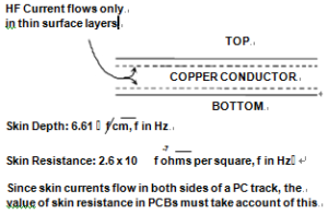
Skin effect is quite a complex phenomenon, and detailed calculations are beyond the scope of this discussion. However, a good approximation for copper is that the skin depth in centimeters is 6.61/√f, (f in Hz). A summary of the skin effect within a typical PCB conductor foil is shown in below Figure.
Skin Depth in a PCB Conductor
Note that this copper conductor cross-sectional view assumes looking into the side of the conducting trace. Assuming that skin effects become important when the skin depth is less than 50% of the thickness of the conductor, this tells us that for a typical PC foil, we must be concerned about skin effects at frequencies above approximately 12 MHz.
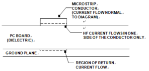
Where skin effect is important, the resistance for copper is 2.6 x 10⁻⁷ √f Ω/square, (f in Hz). This formula is invalid if the skin thickness is greater than the conductor thickness (i.e., at dc or LF). Below Figure illustrates a case of a PCB conductor with current flow, as separated from the ground plane underneath.
Skin Effect with PCB Conductor and Ground Plane
In this diagram, note the (dotted) regions of HF current flow, as reduced by the skin effect. When calculating skin effect in PCBs, it is important to remember that current generally flows in both sides of the PC foil (this is not necessarily the case in microstrip lines, see below), so the resistance per square of PC foil may be half the above value.