

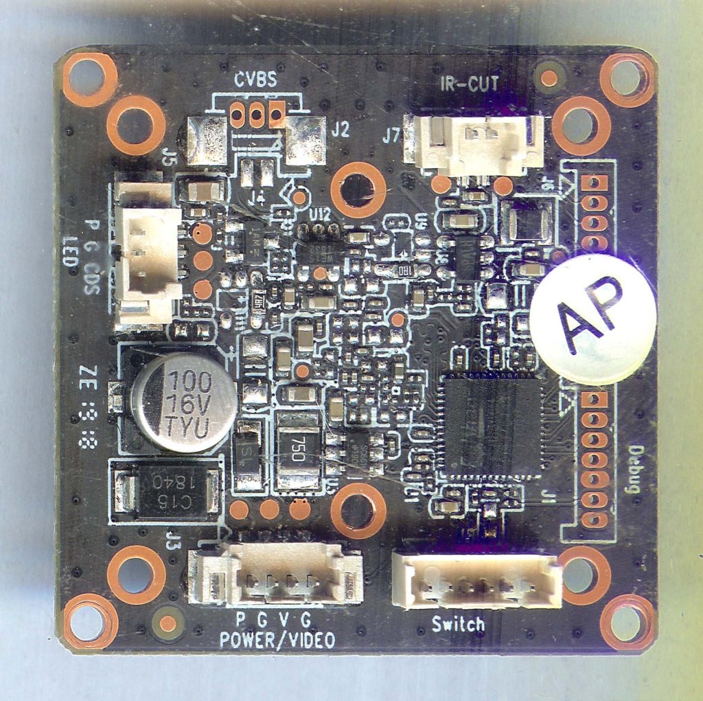
Copying PCB Wiring Card
Copying PCB Wiring Card and re-manufacture the circuit board by scheme diagram, gerber file and component list, the cloned PCB card will provide the exact same functions as original version;
The initial size of new vias may be changed by <Key>v and Shift<Key>v or by selecting the appropriate entry from the Sizes menu. Mod1<Key>v and Mod1 Shift<Key>v do the same for the drilling hole of the via. The statusline is updated with the new values being created, and a via is similar to the other objects. Switch to via-mode by using either the selector button or <Key>F1 then press <Key>] or <Btn1> to create one. <Key>n changes the name of a via.
If you want to create a mounting hole for your board from PCB Reverse engineering process, then you can place a via where you want the hole to be then convert the via into a hole. The conversion is done by pressing !Ctrl<Key>h with the cross hair over the via.
Conceptually it is still a via, but it has no copper annulus. If you create such a hole in the middle of two polygons on different layers, it will short the layers. Theoretically you could arrange for such a hole not to be plated, but a metal screw inserted in the hole would still risk shorting the layers.
A good rule is to realize that holes in the board really are vias between the layers and so place them where they won’t interfere with connectivity. You can convert a hole back into a normal via with the same keystroke used to convert it in the first place.
Some of the functions related to elements only work if both the package layer and the pin layer are switched on. Now that you’re familiar with many of the basic commands, it is time to put the first element on the layout acquired from pcb board reverse engineering. First of all, you have to load data into the paste buffer. There are four ways to do this:
1) load the data from a library
2) load the data from a file
3) copy data from an already existing element
4) convert objects in the buffer into an element
We don’t have any elements on the screen yet nor anything in the buffer, so we use number one. Select lsi from the menu in the library window press <Btn1> twice at the appropriate textline to get the MC68030 CPU. The data is loaded and the mode is switched to pastebuffermode.
Each notify event now creates one of these beasts. Leave the mode by selecting a different one or by <Key>Escape which resets all modes for copy PCB board. The cross hair is located at the mark position as defined by the data file. Rotating the buffer contents is done by selecting the rotate entry of the Buffer menu or by pressing Shift<Key>F3.
The contents of the buffer are valid until new data is loaded into it either by a cut-to-buffer operation, copy-to-buffer operation or by loading a new data file. There are 5 buffers available (possibly more or less if changed at compile time with the MAX_BUFFER variable in ‘globalconfig.h’). Switching between them is done by selecting a menu entry or by Shift<Key>1..MAX BUFFER. Each of the two board sides has its own buffers.
Tags: copying pcb wiring card artwork,copying pcb wiring card bom,copying pcb wiring card component list,copying pcb wiring card design,copying pcb wiring card diagram,copying pcb wiring card gerber file,copying pcb wiring card layout,copying pcb wiring card schematic,copying pcb wiring card software