

Copying High Speed PCB Board EMI/EMC Structure
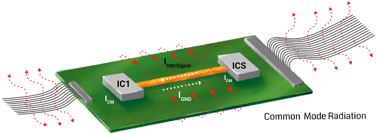
In general, Copying High Speed PCB Board EMI/EMC Structure needs to consider both radiated and conducted aspects. The former belongs to the higher frequency part (>30MHz) and the latter belongs to the lower frequency part (<30MHz).
So you can’t just pay attention to the high frequency and ignore the low frequency part. A good EMI/EMC structure design must take into account the position of the device, the arrangement of the multilayer PCB board stack structure, the way of important connections, the selection of the device, etc. at the beginning of Copying High Speed PCB Board EMI/EMC Structure.
If there is no better arrangement in advance, solving it after the event will get twice the result with half the effort and increase the cost. For example, the position of the clock generator should not be close to the external connector as much as possible. The high-speed signal should go to the inner layer as much as possible and pay attention to the continuity of the characteristic impedance matching and the reference layer to reduce reflection.
The slope (slew rate) of the signal pushed by the device should be as small as possible to reduce high frequency components, When selecting a decoupling/bypass capacitor, pay attention to whether its frequency response meets the requirements to reduce power plane noise.
In addition, pay attention to the return path of the high-frequency signal current to make the loop area as small as possible (that is, the loop impedance as small as possible) to reduce radiation. It is also possible to control the range of high-frequency noise by dividing the formation. Finally, properly select the grounding point (chassis ground) between the PCB and the case.