

Controller PCBA Board Gerber File Cloning
In the Controller PCBA Board Gerber File Cloning, layout of components, components related to each other should be placed as close as possible. For example, clock generators, crystal oscillators, and CPU clock input terminals are prone to noise.
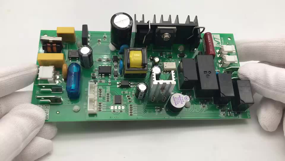
When placed, they should be placed close to each other. For those components that are prone to noise, small-current circuits, high-current circuit switching circuits, etc. should be kept away from single-chip logic control circuits and storage circuits (ROM, RAM) as far as possible. If possible, these circuits can be re-layout into circuit board circuitry diagram, which is conducive to anti-interference and improves the reliability of circuit operation.
Try installing decoupling capacitors design when reverse engineering pcb board next to critical components like ROM and RAM chips.
In practice, Controller PCBA Board Gerber File Cloning for pin routing and routing may contain large inductive effects. Large inductances can cause severe switching noise spikes in the Vcc routing. The only way to prevent switching noise spikes in the Vcc routing is to place a 0.1uF electronic decoupling capacitor between Vcc and the source.
If a surface mount component is used on the pcb board, a chip capacitor can be placed directly against the component and connected to the Vcc pin. Tile capacitors are preferred because of their low ESL electrostatic losses, high frequency impedance, and good dielectric stability over temperature and time. Tantalum capacitors should not be used as much as possible due to their high impedance at high frequencies.