

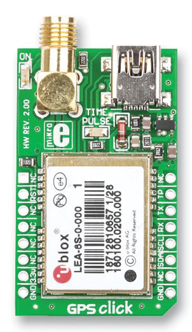
Clone GPS Navigation PCB Board
As the demand for location-based services grows across transportation, aviation, marine, and military sectors, GPS navigation PCB boards remain at the heart of many embedded systems. However, many legacy GPS devices are reaching their end-of-life stage, and support from OEMs has either ceased or become too costly. For companies and individuals relying on these technologies, the ability to clone a GPS navigation PCB board offers a strategic way to extend the life of existing systems, refurbish hardware, or even innovate upon proven designs.
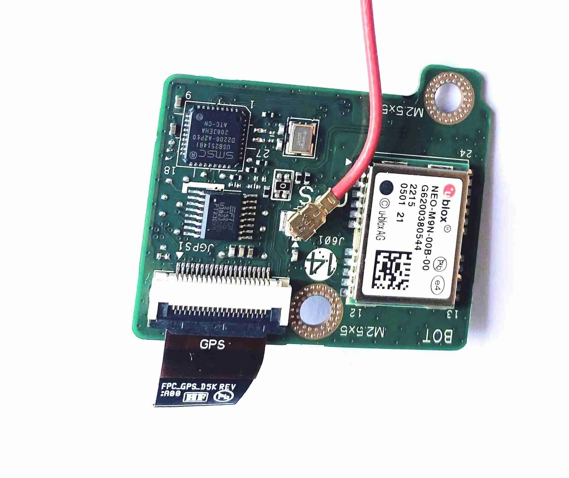
What Makes a GPS Navigation PCB Unique?
Cloning a GPS navigation PCB board is far more complex than duplicating a standard control board. These PCBs are typically multi-layered, often featuring RF circuits, signal filtering paths, and high-precision timing components. The layout must minimize interference, maintain impedance control, and integrate specialized ICs like GPS modules, microcontrollers, power management chips, and occasionally real-time kinematic (RTK) systems for enhanced accuracy.
Moreover, the inclusion of sensitive analog and digital signals demands precise layout drawings and carefully tuned netlists to ensure signal integrity. Minor discrepancies in design can lead to performance degradation or complete malfunction, making PCB reverse engineering for GPS boards a demanding task.
The Process of Cloning a GPS Navigation PCB Board
To successfully clone, replicate, or duplicate a GPS navigation PCB, the process begins with high-resolution imaging and layer-by-layer analysis of the physical PCB. Our engineers then:
- Recover and map the trace patterns and via structures.
- Restore the full schematic diagram from the observed circuit logic.
- Generate accurate Gerber files and netlists to match the original electrical performance.
- Build a complete BOM list, including sourcing hard-to-find GPS receiver chips or filters.
- Conduct layout recreation to mirror impedance-sensitive tracks and RF shielding areas.
This data is then compiled into a complete engineering package, allowing for seamless reproduction or remanufacture of the original board.
Challenges in Reverse Engineering GPS Navigation PCBs
- Miniaturization: Many GPS PCBs use compact, high-density designs to save space, making trace recovery a delicate process.
- Proprietary Components: Some modules or chips may be discontinued or obscured, requiring redevelopment or redesign around alternative parts.
- RF Sensitivity: Rebuilding a layout without proper RF consideration can result in significant signal drift or loss.
- Multilayer Complexity: Blind/buried vias and internal layers are difficult to detect and map without advanced equipment.
These challenges require both specialized tools and skilled engineers experienced in reverse engineering, refurbishment, and redesign of RF and navigation-grade electronics.
Strategic Value to Businesses and Engineers
The ability to clone a GPS navigation PCB board provides significant strategic advantages. For manufacturers, it enables the redevelopment of discontinued modules. For system integrators and maintenance teams, it ensures continuity in fleet or mission-critical applications where replacing the entire unit is not feasible. For engineers, it’s an opportunity to copy and improve upon proven legacy systems with modern enhancements.
In all cases, rebuilding the obsolete documents such as Gerber files, schematic diagrams, and BOM lists is essential to supporting long-term operational readiness.
Clone GPS Navigation PCB Board project will be able to provide all the necessary files for PCB board copying include Layout drawing, BOM, Gerber file and schematic diagrams, submited in below format through which your PCB board can be manufacture and assembly anywhere in the world, we can ensure the accuracy of your data by means of prototype running.
Here is sample of files and drawings you will receive, based on a typical double layer GPS Navigation PCB Board Clone with components mounted on two sides:
BOTTOM Layer of GPS Navigation PCB Board:

TOP Layer of GPS Navigation PCB Board:

SCHEMATIC DIAGRAM of GPS Navigation PCB Board:

Circuit Engineering Company Limited provide a complete PCB Reverse Engineering, PCB Clone and PCB Restoration service, Rapid Prototyping and functional test services using the latest technologies combined with traditional skills for a wide range of industries. By integrating our traditional skills with the latest technologies, we can offer clients a comprehensive portfolio of product development services all under one roof. For more details please contact our customer
service team.
Conclusion
Recreating legacy GPS technology isn’t just about copying—it’s about understanding the intricacies of a precision navigation system and rebuilding it with modern accuracy. Our advanced methods to clone a GPS navigation PCB board ensure performance, reliability, and long-term usability. Whether you need a one-time reproduction or plan to remanufacture in volume, we can recover what was lost—and rebuild it better.