

Circuit Board Design File Reverse Engineering
The basic knowledge of Circuit Board Design File Reverse Engineering is applicable to both analog and digital circuits. A basic rule of thumb is to use an uninterrupted ground plane. This common sense reduces the dI/dt (change in current with time) effect in digital circuits, which changes the ground potential and causes noise to enter analog circuits.
The reverse engineering pcb card techniques for digital and analog circuits are basically the same, with one exception. For analog circuits, there is another point to note, that is, keep the digital signal lines and loops in the ground plane as far away from the analog circuits as possible.
This can be achieved by connecting the analog ground plane to the system ground connection separately, or placing the analog circuit at the farthest end of the circuit board, which is the end of the line. This is done to keep the external interference on the signal path to a minimum.
This is not necessary for digital circuits, which can tolerate large amounts of noise on the ground plane without problems;
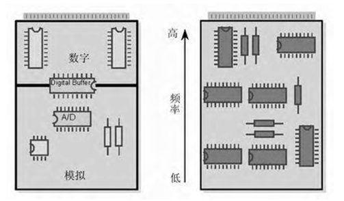
(a) Isolate the digital switching action from the analog circuit, and separate the digital and analog parts of the circuit. (b) Separate high frequency and low frequency as much as possible, and the high frequency components should be close to the connectors of the circuit board