

Buffering ADCs Against Logic Noise
Buffering ADCs Against Logic Noise
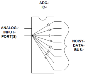
Today we are going to talk about the Buffering ADCs Against Logic Noise, If we have a high resolution data converter (ADC or DAC) connected to a high speed data bus which carries logic noise with a 2 V/ns to 5 V/ns edge rate, this noise is easily connected to the converter analog port via stray capacitance across the device. Whenever the data bus is active, intolerable amounts of noise are capacitively coupled into the analog port, thus seriously degrading performance.
A High Speed ADC IC Sitting on a Fast Data Bus Couples Digital
This particular effect is illustrated by the diagram of above Figure, where multiple package capacitors couple noisy edge signals from the data bus into the analog input of an ADC.
Present technology offers no cure for this problem, within the affected IC device itself. The problem also limits performance possible from other broadband monolithic mixed signal ICs with single chip analog and digital circuits. Fortunately, this coupled noise problem can be simply avoided, by not connecting the data bus directly to the converter.
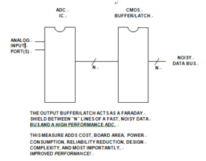
Instead, use a CMOS latched buffer as a converter-to-bus interface, as shown by below Figure. Now the CMOS buffer IC acts as a Faraday shield, and dramatically reduces noise coupling from the digital bus. This solution costs money, occupies board area, reduces reliability (very slightly), consumes power, and it complicates the design—but it does improve the signal-to-noise ratio of the converter!
The designer must decide whether it is worthwhile for individual cases, but in general it is highly recommended.
A High Speed ADC IC Using a CMOS Buffer or Latch at the Output