

Blind and Buried Vias in PCB Board Layout File Cloning
Blind and Buried Vias in PCB Board Layout File Cloning are most commonly seen in the high density interconnect circuit board, Blind vias are vias that connect the surface and inner layers without penetrating the entire PCB board.
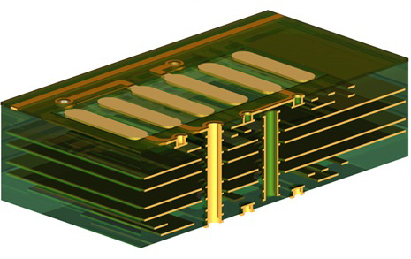
Buried vias are through holes that connect the inner layers and are not visible on the surface of the finished printed circuit board. For the size settings of these two types of vias.
When applying blind hole and buried hole of reverse engineering printed circuit card design, you should have a full understanding of the PCB processing process to avoid unnecessary problems in PCB processing, and negotiate with the PCB supplier when necessary.
Test hole
Test holes refer to pcb board reverse engineering vias used for ICT testing purposes, which can also be used as via holes. In principle, the aperture is not limited, the diameter of the pad should be no less than 25mil, and the center distance between the test holes should not be less than 50mil.
It is not recommended to use component solder holes as test holes