Analog and Digital PCB Circuit Reverse Design against Noise
In every Analog and Digital PCB Circuit Reverse Design against Noise, the noise part of the circuit and the “quiet” part (non-noise part) should be separated.
Generally speaking, digital circuits are “rich” in noise and are insensitive to noise (because digital circuits have a large voltage noise tolerance);
In contrast, the voltage noise tolerance of analog circuits is much smaller. Of the two, analog circuits are the most sensitive to switching noise. In the wiring of a mixed-signal system, these two circuits should be separated.
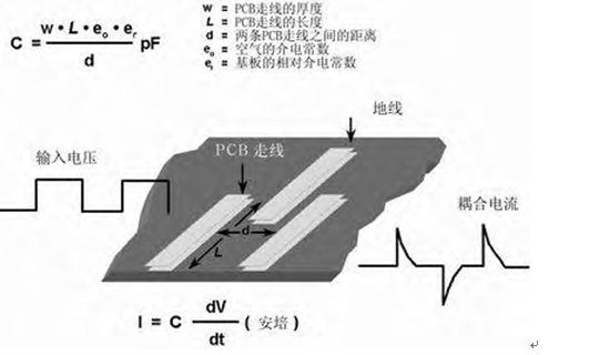
Placing two close traces on the digital PCB board circuitry drawing reverse engineering process can easily form parasitic capacitance. Due to the existence of this kind of capacitance, a rapid voltage change on one trace can generate a current signal on the other trace, see below pictures:
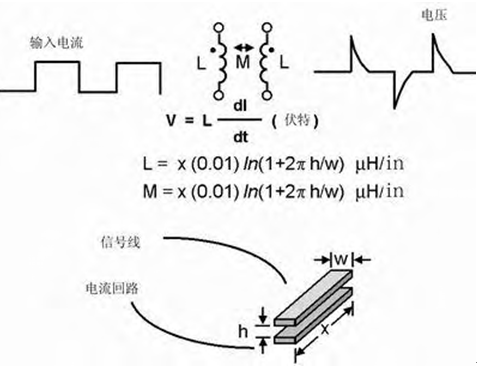
If you do not pay attention to the placement of the traces, the traces in the PCB may produce line inductance and mutual inductance. This parasitic inductance is the location of components that are very harmful to the operation of circuits containing digital switching circuits.