

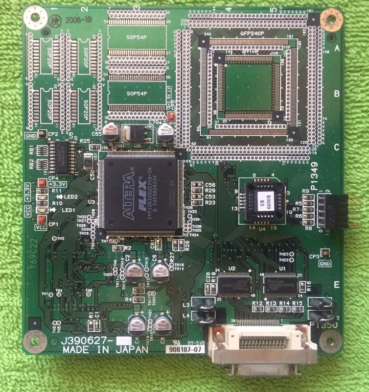
Altera’s LVDS System PCB Board Design Cloning
LVDS is a high-speed, low-voltage, low-power, and low-noise general-purpose I/O interface standard. The low voltage swing and differential current mode output significantly reduces electromagnetic interference (EMI). These outputs have faster edge rates, allowing the signal path to function as a transmission line. Therefore, ultra-high-speed Altera’s LVDS System PCB Board Design Cloning and differential signaling theory are useful for designing boards that incorporate Altera FPGAs and integrate LVDS. In addition, when reverse engineering an LVDS circuit board schematic diagram and layout drawing, there are various factors to consider such as differential traces, impedance matching, crosstalk, and EMI.
LVDS uses a differential transmission mechanism, and each LVDS signal uses two traces. The voltage difference between these two traces defines the LVDS signal value. When copying the layout and gerber file of the pcb board, follow the guidelines below to successfully transmit LVDS signals on the differential traces.
To minimize reflections and maintain common-mode noise rejection of the receiver, the differential lines should be placed as close to each other as possible after leaving the driver IC. Also, to avoid discontinuities in the differential impedance, the distance between the differential LVDS signals should remain constant throughout the trace.
To reduce skew, the electrical signal lengths between differential LVDS traces should be the same. The arrival of one signal before the other creates a phase difference between the signal pairs, reducing the receiver skew margin (RSKM) and thus affecting system performance.
Reduce the number of vias or other discontinuities on the signal path. Any stray loads such as capacitors must be the same size on each trace of the differential pair. To avoid signal discontinuities, a 45° arc trace is recommended instead of a 90° right angle turn.
Tags: clone o design da placa PCB do sistema LVDS da Altera,copie o design da placa PCB do sistema LVDS da Altera,engenharia reversa do projeto da placa PCB do sistema LVDS da Altera