

AC Driver Circuit Board Reverse Engineering
AC Driver Circuit Board Reverse Engineering
The first conventional AC Driver Circuit Board Reverse Engineering places the input capacitors and devices on the same side of the PCB in close proximity to minimize the size of the high frequency loop [2]. The high frequency loop for this layout is contained on the same side of the PCB and is considered a lateral power loop as a result of the power loop flowing on the board plane on a single layer.
An eGaN FET design arranged in a lateral power loop was created and the part placement and high frequency power loop are shown in figure 4 with the high frequency loop highlighted (a) (b) in red.
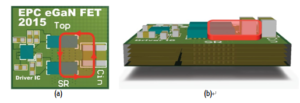
For this design, the inductor connection is made through internal layers using vias in between the top switch and synchronous rectifier. The driver is located in close proximity to the eGaN FETs to minimize common source inductance and keep the common source inductance constant between designs. This allows a comparison of only the influence of high frequency loop inductance.
While minimizing the physical size of the loop is important to reduce parasitic inductance, the design of the inner layers is also critical. For the lateral power loop design of the AC Driver Circuit Board Reverse Engineering, first inner layer serves as a “shield layer”.
AC Driver Circuit Board Reverse Engineering
This layer has a critical role to shield the circuit from the fields generated by the high frequency power loop. The power loop generates a magnetic field that induces a current, opposite in direction to the power loop, inside the shield layer.
The current in the shield layer generates a magnetic field to counteract the original power loop’s magnetic field. The end result is a cancellation of magnetic fields that translates into a reduction in parasitic inductance at the cost of increased eddy current losses within the shield. Having a complete shield plane in close proximity to the power loop provides the best performance.