

PCB Reverse Engineering Software
PCB reverse engineering is a sophisticated process that involves extracting technical data from an existing printed circuit board (PCB) to recover, reproduce, or redesign the original product. Whether the goal is to restore a legacy board, recreate a schematic diagram, or remanufacture an obsolete component, specialized software plays a vital role in the workflow. These tools help engineers copy, replicate, or duplicate the original design accurately, while also allowing for in-depth analysis and potential improvement.
- Introduction to PCB Reverse Engineering Software
Modern PCB reverse engineering relies heavily on advanced software to extract, interpret, and recreate data. These tools are used to generate or manipulate essential files such as Gerber files, netlists, BOM lists (Bill of Materials), and layout drawings. The software also assists in visualizing and rebuilding the schematic diagram, making it easier to refurbish or redevelop a product for continued use or new applications. - Key Software Used in PCB Reverse Engineering
a. Altium Designer
Altium is one of the most widely used platforms for PCB design and reverse engineering. Its capabilities allow engineers to import Gerber files, reconstruct netlists, and generate layout drawings. Altium’s powerful schematic capture tools make it ideal for recovering and recreating schematic diagrams, especially when integrated with its library of electronic components.
b. KiCad
An open-source alternative, KiCad is widely used for budget-sensitive projects. It supports Gerber file editing, schematic recreation, and layout generation. Although it may lack some of the premium features found in commercial platforms, it remains highly effective for basic to moderately complex PCB duplication and redevelopment tasks.
c. EasyEDA
This web-based tool is convenient for reverse engineering, especially when dealing with BOM lists, schematics, and Gerber files. It allows direct import and manipulation of PCB data, making it useful for quick restoration or modification projects.
d. CAM350
CAM350 is primarily used for Gerber file analysis and editing. It’s particularly valuable in the remanufacturing process, where understanding and validating production files is critical. Engineers use CAM350 to verify layer alignments, trace routing, and ensure manufacturability during reverse engineering.
e. Xpedition and PADS by Siemens
These high-end tools are tailored for complex, multilayer PCBs found in aerospace, medical, or defense sectors. With advanced simulation and verification tools, they are ideal for reproducing high-frequency circuit boards, validating netlists, and ensuring exact matches during PCB cloning and redesign.
f. DesignSpark PCB
DesignSpark PCB offers free schematic capture and PCB layout capabilities. It supports BOM export, netlist recovery, and layout duplication, which is great for refurbishing or upgrading simpler boards.
- Integrated Reverse Engineering Workflow
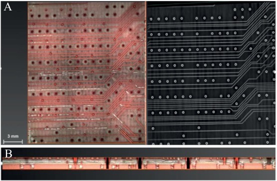
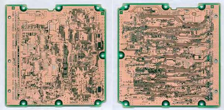
The reverse engineering process usually starts with scanning or photographing the physical PCB to create a digital image. From there, software tools are used to trace circuit paths, identify component footprints, and recreate the schematic diagram. The resulting netlist is compared against the physical layout to ensure accuracy. Next, the Gerber files and BOM list are generated to support remanufacture or redevelopment. Advanced tools even allow simulations to verify electrical behavior before building a prototype.

PCB Reverse Engineering Software
For PCB Reverse Engineering software, PROTEL 99se is a CAD software launch in the end of 1980 which is the first choice as PCB Reverse Engineering Software. PROTELL 99se is being used in domestic market early and the population rate is high. Some university and colleague even install course for the study and research on this software. Almost all the electronic design company will apply it. It was used as automatic routing tools for printed circuit board at the early stage which is run under DOS system and has low requirement on the hardware. If there is only electronic schematic diagram and PCB design function, then the automatic routing success rate could be low. Now PROTEL has already developed to PROTEL 99se which is a huge EDA software, it include schematic diagram drawing, analog circuit and digital circuit combination signal simulation, multilayer circuit board design, programmable logic semiconductor design, drawing generation and etc.
Whether all the jobs can be done completely within the same software is an critical element to judge if it is good for PCB Reverse Engineering, for this point PROTEL 99se can be viewed a good choice because two reasons:
1 It is component library is rich and can be downloaded from internet freely;
2 Define the network grid is required to spread the copper on the circuit drawing, for complicate Printed circuit board, there is lots of connection and separation on the copper area.