

Reverse Engineering PCB India
Reverse Engineering PCB in India: Unlocking Innovation in the Electronics Sector
The electronics industry in India is experiencing a transformative phase, driven by rapid technological advancements and a growing emphasis on self-reliance. Within this landscape, Reverse Engineering of Printed Circuit Boards (PCBs) has emerged as a critical practice, enabling businesses to innovate, repair legacy systems, and stay competitive. This article explores the significance, applications, challenges, and opportunities of PCB reverse engineering in India.
What is PCB Reverse Engineering?
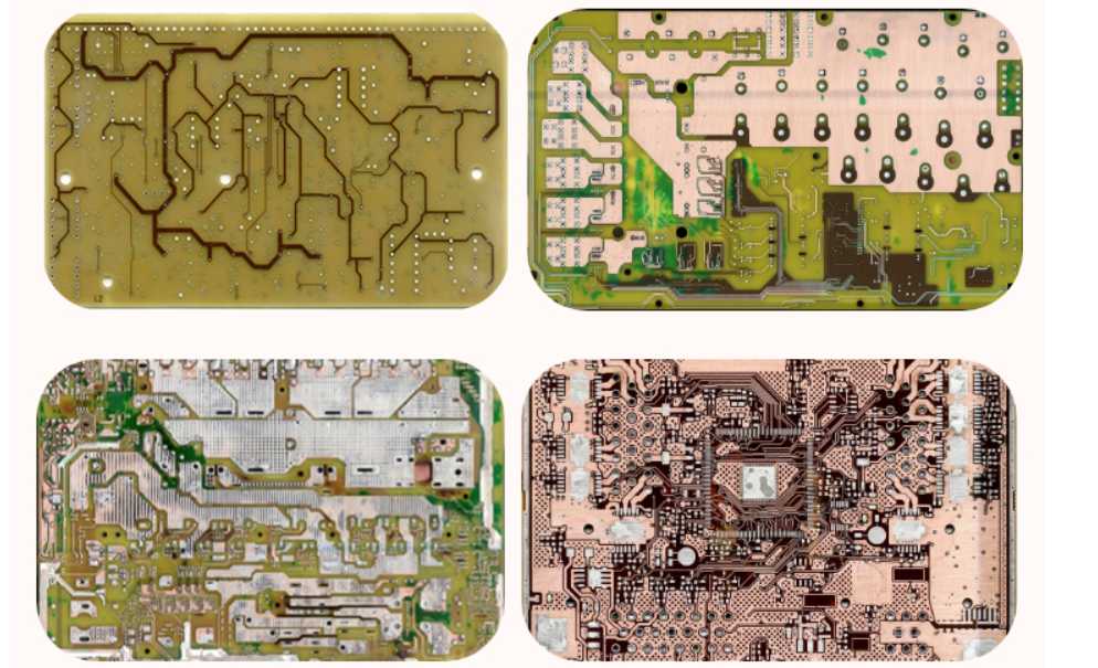
Reverse engineering PCBs involves deconstructing an existing circuit board to understand its design, components, and functionality. This process is essential when original documentation is unavailable, or when companies need to upgrade outdated systems, troubleshoot failures, or analyze competitors’ products. Techniques such as X-ray imaging, chemical etching, and 3D scanning are often used to recreate schematics and identify component layouts.
Why India?
India’s electronics manufacturing sector, valued at over $100 billion, is poised to grow exponentially under initiatives like Make in India and the Production-Linked Incentive (PLI) Scheme. As domestic demand for consumer electronics, automotive electronics, and defense equipment rises, reverse engineering has become a strategic tool for:
- Legacy System Maintenance: Many industries rely on outdated machinery with obsolete PCBs. Reverse engineering helps recreate or repair these boards, extending equipment lifespan.
- Localized R&D: Companies use reverse engineering to study global technologies and adapt them to local needs, reducing dependency on imports.
- Defense & Aerospace: Critical for analyzing foreign technology or refurbishing legacy systems in a sector where transparency is limited.
Key Applications
- Consumer Electronics: Repairing devices like smartphones and IoT gadgets.
- Automotive: Adapting PCB designs for electric vehicles (EVs) and connected cars.
- Industrial Automation: Modernizing manufacturing equipment.
- Medical Devices: Ensuring compliance and safety in life-saving equipment.
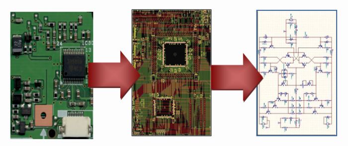
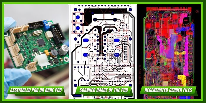
The Reverse Engineering Process
- Imaging & Scanning: High-resolution imaging captures PCB layers.
- Component Analysis: Identifying and testing ICs, resistors, and connectors.
- Schematic Recreation: Using CAD tools to map circuitry.
- Prototyping & Testing: Validating the cloned PCB’s functionality.
Challenges in India
- Ethical & Legal Concerns: Balancing innovation with intellectual property (IP) rights. Reverse engineering for cloning without authorization can lead to legal disputes.
- Technical Complexity: Multi-layered PCBs and miniaturized components (e.g., BGA chips) require advanced tools and expertise.
- Skill Gaps: While India has a strong engineering talent pool, specialized training in reverse engineering is limited.
Opportunities Ahead
India’s push for Atmanirbhar Bharat (Self-Reliant India) is accelerating investments in R&D infrastructure. Startups and MSMEs are leveraging reverse engineering to develop affordable alternatives to imported electronics. Educational institutions are also collaborating with industries to bridge skill gaps. Cities like Bengaluru, Hyderabad, and Pune are becoming hubs for PCB design and innovation.
Conclusion
Reverse engineering PCBs is not just about replication—it’s a gateway to innovation, enabling India to strengthen its electronics ecosystem. By addressing ethical concerns and investing in cutting-edge tools and training, India can position itself as a global leader in PCB design and manufacturing. As the sector evolves, reverse engineering will remain a cornerstone of sustainable technological progress, driving the nation toward a future of electronics self-sufficiency.
As we know that Reverse Engineering PCB India final purpose is to produce an workable functional prototype which possess the same or more advanced technology. Then Post-shipment inspection can preclude the replication of defects, the hardware provided for pcb reverse engineering should be inspected for possible damage in shipment.
The necessary documentation for control such as Damage Reports or Failed Item Reports, should be generated as required. An initial operating test should be performed to ensure the item functions in accordance with established performance specifications.
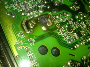
Pre-disassembly photographs, The hardware should be photographed prior to and during disassembly since, in some cases, no other record of the item exists. In addition, since the piece-parts will be identified by bagging and tagging, their position in the assembly should be noted.
Tags: PCB Reverse Engineering china,PCB Reverse Engineering india,PCB Reverse Engineering uk