

Screen of Radio Frequency Circuit from PCB Card Cloning
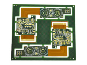
Radio Frequency Circuit from PCB Card Cloning
The concept of wireless transmitter and receiver from pcb card cloning can be categorize into two parts, base frequency and radio frequency. Basic frequency will include the input signal’s frequency range, as well as the frequency range of output signals from the receiver. The frequency width of the basic frequency determine the basic rate data can flow into the system; basic frequency will be used to optimize the reliability of the data flow, and reduce the transmission medium overload executed by transmitter. As a result of that, when design the basic frequency circuits, need great amount of signal processing knowledge and great amount of experience on pcb card cloning.
The radio frequency circuit from transmitter can convert and upgrade the basic frequency signal into the subscribed channel and at the same time inject the signal into the transmission media. On the contrary, the radio frequency circuit of receiver can obtain the signals from the transmission media when pcb card cloning, through conversion and degradation to basic frequency.
The two main targets of the pcb card cloning design from Radiator includes, first of all, in the pretext of minimum power consumption, there is specified power rate to be radiated. Secondly, it won’t interfere the adjacent channels operation. As for the receiver, there are three main subjects: first of all, they must restore small signals precisely; secondly, they must be able to eliminate the interference signals beside expected channels after cloning pcb card; the last point is same as the radiator, the power consumption of them must be very small.