

Reverse Engineering Printed Circuit Board Outline
Reverse Engineering Printed Circuit Board needs to take the outline and component layout into consideration, first of all, the size of electronic PCB board outline must be adapt to the moderate standard, if the size of PCB is too large, which will increase the length of circuit conductor length after PWB Cloning, and make rise to the impedance as a result, it will not only drop the anti-noise capability to the low level, but also increase the PCB board manufacturing budget;
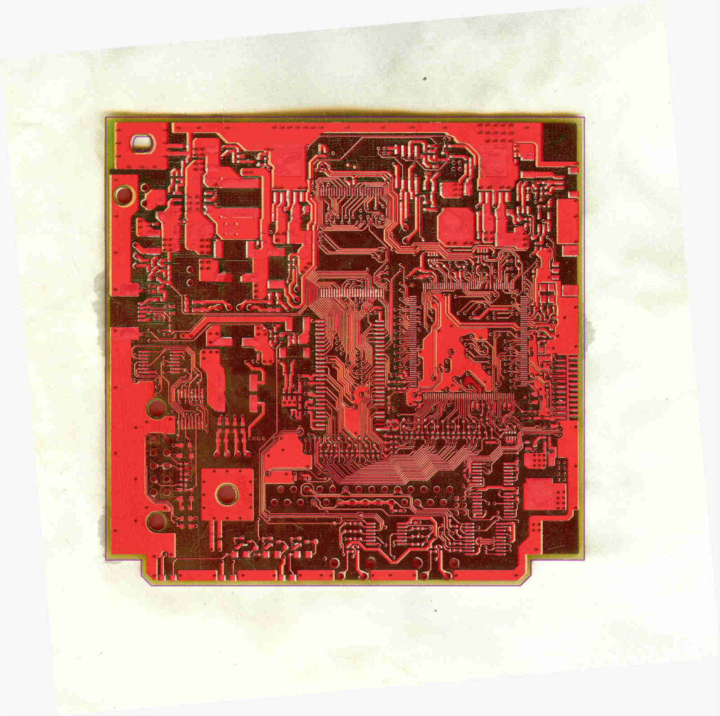
However, if the dimension of PCB board is too small, it can cause the poor performance on the thermal dissipation and more apt to be disturbed by the adjacent conductors. It has almost the same principle compare with other logical circuit, and engineers should put the interact components as close as possible on the drawing acquired from PCB card cloning which can obtain better result for the anti-noise interference effect.
Others like clock generator, crystal oscillator, and input terminal of CPU clock can generate noise easier, so these components should be placed as close as to each other to bring down the noise. There are also other components which are easier to generate the noise include low current, big current circuit should be placed away from the logic circuit.
Tags: replicating circuit board,replicating circuit card,replicating pcb,replicating pcb assemble,replicating pcb board,replicating pcb card,replicating pcba,replicating printed circuit board,replicating printed wiring board,replicating pwb,replicating pwba