

Reverse Engineering Printed Circuit Board Digital Wiring
Reverse engineering printed circuit board digital wiring will refers to the mixed signals issue, especially for the current electronic consuming products, most of them have the mixed signals on the separated area and PCB designer should be aware of this point.
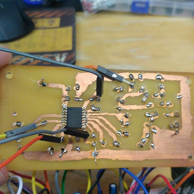
As we all know, Reverse engineering electronic pcb board with mixed signal circuit which include digital circuit and analog circuit could be extremely complicate compare with other PCB reverse engineering.
The electronic component arrangement, PC board layout as well as the power supply and grounding line treatment can directly affect the electrical performance and electro-magnetic performance. So the engineers will sufficient experience can optimize the mixed signal circuit board reverse engineering and design features through the separation of ground and power supply circuit.
Under these three condition, some medical facility has requirement on the leaking current value go through circuit system; and some industry process control facility might have extremely high output with large noise and high power consumption, there is also another case is when redesign the layout of printed circuit board has been restricted under specified situation.
In the mixed signal PCB board layout, there is some isolated digital and analog power supply, it is able to suppose to cut off the power supply layer. However, the signal line which adjacent to the power source layer won’t cross the space between power supplies, and all of the signal lines which cross the space should be located on the circuit layer which has large area of copper. In this situation, design a analog power source in the format of electronic card connecting line instead of a surface can avoid the splitting issue on the power supply side.
Tags: reverse engineering circuit board,reverse engineering circuit card,reverse engineering pcb,reverse engineering pcb assemble,reverse engineering pcb board,reverse engineering pcb card,reverse engineering pcba,reverse engineering printed circuit board,reverse engineering printed wiring board,reverse engineering pwb,reverse engineering pwba