

Reverse Engineering PCB Wiring Card
Reverse Engineering PCB Wiring Card is a reverse order of Printed circuit board manufacturing, the PCB board will be delayer after all the assembled electronic components removed from it;
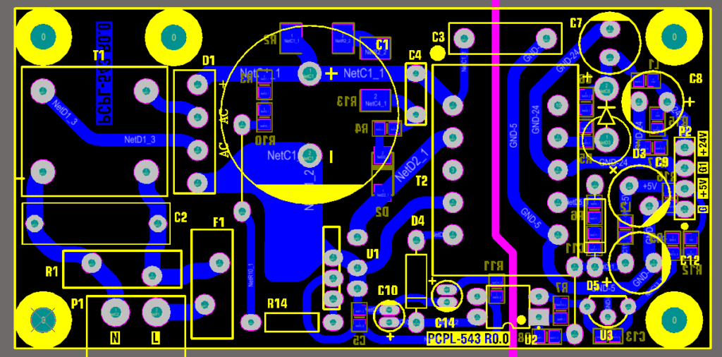
Selection of PCB Raw Material for PCB manufacturing by choosing the gerber file from printed circuit board reverse engineering layout
Base material include the organic and non-organic types, and the most important factors when selecting raw material is dielectric constant, dissipation constant, thermal expansion parameter and moisture absorption parameters. Among them the dielectric constant will affect the track impedance and signal transmission rate when cloning printed circuit. for the high frequency circuit, the tolerance of dielectric constant is the one factor which should be taken into consideration, so PCB wiring card should choose the raw material with low dielectric constant.
2, PCB board design Procedure
Due to the application of Protel 99se software and its difference with Protel 98, as a result of that, it is necessary to discuss PCB board copying by using Protel 99se.
1> Since the Protel 99se use PROJECT database model management, so it is necessary to establish a database file to manage all of the PCB wiring card schematic diagram and Layout;
2> Schematic diagram of PCB wiring card: in order to achieve the network connection, before proceed the schematic diagram design, all of the components used on the PCB wiring card must be able to be found from the electronic database, otherwise, designer should design the required components and store these parts into the database in advance. After that, designer just need to use the required components from it, and make the electrical connection according to the schematic diagram;
3> After the completion of PCB wiring card schematic diagram has been done, it will form a network list which can be used for the PCB card cloning usage.
4> Layout printed circuit board: a, confirm the pcb wiring card dimension and outline, PCB wiring card electronic components quantity and definite its location, required space in the finished product, shape as well as the cooperation with other components.
a; Use the PLACE TRACK order to draw the pcb wiring card outline in the mechanical layer.
b; according to the surface mount technology requirement to make the tooling hole and reference point on the PCB wiring card;
c; the component layout and placement;
Tags: reverse engineering circuit board,reverse engineering circuit card,reverse engineering pcb,reverse engineering pcb assemble,reverse engineering pcb board,reverse engineering pcb card,reverse engineering pcba,reverse engineering printed circuit board,reverse engineering printed wiring board,reverse engineering pwb,reverse engineering pwba