

Reverse Engineering PCB Board Service Procedures
Reverse Engineering PCB Board Service Procedures
PCB Board , are ubiquituous. PCB Boards are the backbones of almost every electronic device, and therefore, Reverse Engineering PCB Board and manufacturing are extremly important compozsnents of many industrial production processes.
Before a Printed circuit board can be re-manufactured according to the original samples, it evolves through three main steps. The first one is to desolder the components off Printed circuit board, which defines the components to be used and their interconnections.
The second step is the draw layout of the Printed circuit board where the geometric positions of the components and their physical connections are decided. The final step is the industrial production of the PCB.
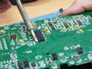
first step of reverse engineering pcb board- desolder component off pcb
In this article we give an overview on the mathematical models and methods used in the second step, the physical reverse engineering of the board. The two major issues here are component placement and wire routing as depicted in below Figure.
A digital logic circuit consists of a collection of interconnected parts. The parts come in two varities;
active parts, i. e., integrated circuits (IC) and passive parts, such as resistors, and capacitors (Figure 2).
Due to continuously shrinking feature sizes, the functionality of ICs per area unit has significantly increased over the years. This has led to a steady increase of the ratio between passive and active parts of a PCB as well as the difficulty of reverse engineering PCB board. Ratios of 20 or 30 passive to one active part are not uncommon. Each part can be represented by the shape and area occupied on the board together with the locations of one or more pins or pads where the electrical connections are made after Printed circuit board clone. One IC may have up to several hundred pins.