

Reverse Engineering Electronic PCB Board
Reverse Engineering Electronic PCB Board will refers to the mixed signals issue, especially for the current electronic consuming products, most of them have the mixed signals on the separated area and Electronic pcb board designer should be aware of this point.
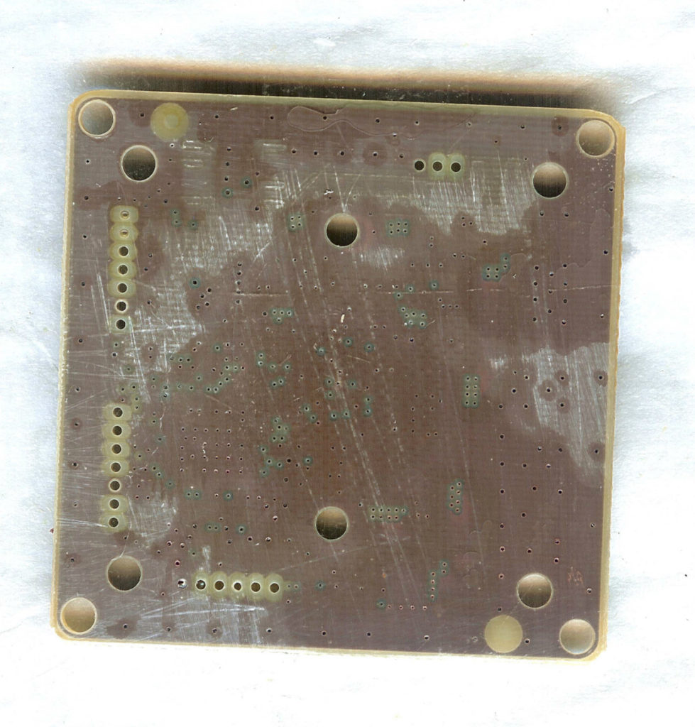
As we all know, Electronic pcb board with mixed signal circuit which include digital circuit and analog circuit could be extremely complicate compare with other Circuit board schematic diagram.
The electronic component arrangement, Electronic pcb board layout as well as the power supply and grounding line treatment can directly affect the electrical performance and electro-magnetic performance. So the engineers with sufficient experience can optimize the mixed signal Electronic pcb board design features through the separation of ground and power supply circuit.
Redesign Electronic pcb board with mixed signals is a long and complicate process, during which we should pay attention to below points:
1, separate the Electronic pcb board into isolated analog part and digital part;
2, proper electronic components on the Electronic pcb board;
3, Alternative and DIRECT current convertor for placement;
4, don’t separate the ground, layout united grounds among the digital part and analog part;
5, in all of the layers of Electronic pcb board, digital signals can only be layout on the digital part of Electronic PCB Board;
6, in all of the layers, analog signals can only be layout on the analog part;
7, separation of digital and analog power supply cut off;
8, the circuit shouldn’t be layout cross the space between power supply layers;
9, those signals line which need to cross the power sources should be adjacent to the layer which has large copper area;
10, analyze the actual route and way of revert current;
11, use the right way to layout Electronic pcb board;
Tags: pcb assemble reverse engineering,pcb board reverse engineering,pcb card reverse engineering,pcb circuit board reverse engineering,pcb reverse engineering,pcba reverse engineering,Printed Circuit Board Reverse Engineering,printed wiring board reverse engineering,pwb reverse engineering,pwba reverse engineering