

Printed Wiring Board Replication Skill
Printed Wiring Board Replication Skill needs the engineer to familiar with chemical solution, because it is needed to remove the soldering paste, and equipped with electronic knowledge about reverse engineering PCB board layout, designing and finally PCB card manufacturing capability;
When reverse engineering printed circuit board, especially the multilayer PCB, it is a very time and energy consuming work, which includes great amount of repetitive work. And designer must have sufficient patience and carefulness, otherwise it can lead to mistake. And the key to make a good Printed wiring board cloning job is using a proper software to substitute manpower for these repetitive work which can save both time and improve the correctiveness.
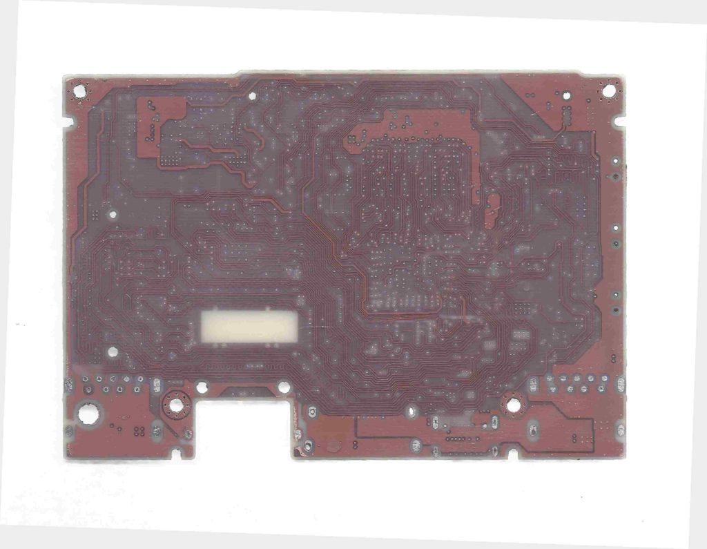
1> Scanning machine must be used in the process of PCB replication, most of the designer get used to draw line on the PCB design system such as PROTEL, PADSOR or CAD. This is a bad habit, since the scanning file can not only be the basis for the PCB file conversion, but also evidence of inspection after Printed wiring board cloning completeness. Use the scanning device can greatly decrease the labor difficulty and strength. Without any exaggeration, use the scanning device properly, even a person without sufficient design experience can complete work;
2> Scrubbing Printed wiring board from single direction, some of the designer will scrub the PCB from dual direction for the sake of faster scrubbing speed, it is a wrongdoing, since the dual direction scrubbing can easily damage the printed wiring board and cause the destruction spread to other layer which can bring the fatal damage to the whole process. And external layer of PCB could be the toughest layer among all of the layers due to surface treatment, copper foil thickness and soldering pad, internal layer has the maximum softness, and normally in the most internal layer, the problem could be more severe since this layer could be too thin to undertake any scrubbing. Besides, due to the variations of Printed wiring board base laminate, thickness and flexibility from various manufacturers, it will add more difficulty.
3> Choose the excellent conversion software, convert the scanned PCB drawing into PCB layout or Gerber is the key for Printed wiring card reverse engineering success, with the good conversion file, designer just need to draw the PCB according to these scanning files, and hereby we recommend to use the EDA2000.
Tags: replicate circuit board,replicate circuit card,replicate pcb,replicate pcb assemble,replicate pcb board,replicate pcb card,replicate pcba,replicate printed circuit board,replicate printed wiring board,replicate pwb,replicate pwba