Printed Circuit Board Reverse Engineering Technology
PCB reverse engineering is the process of recovering, restoring, and recreating the full technical documentation and design of a PCB from a physical sample. With advanced tools and methodologies, engineers can duplicate, clone, or remanufacture a PCB even when all original design files have been lost. This includes:
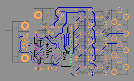
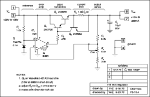
- Creating accurate schematic diagrams that reflect the original circuit’s functionality
- Generating Gerber files required for fabrication
- Producing layout drawings for visual reference or future redesign
- Extracting complete BOM lists (Bill of Materials) for sourcing components
- Developing a netlist for electrical connectivity verification
The entire process makes it possible to reproduce even highly complex, multilayer PCBs with precision.
Printed Circuit Board Reverse Engineering Technology also needs to apply the PCB card layout design skill since the schematic diagram restoration process is going to take by after PCB layout has been drawn;
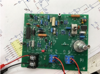
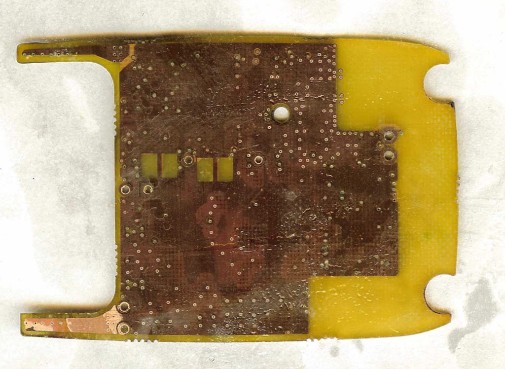
Printed circuit board duplicating engineering is a populated technology and has been widely accepted by most of the nations for the reverse engineering industry field. All printed circuit board need to cleaned before reverse engineering it, so it becomes quite indispensible step to find the most effective way to clean it, hereby we would like to introduce a way for clean printed circuit board cloning:
For businesses maintaining older systems in aerospace, medical, industrial, or defense sectors, the inability to replace or repair a critical board due to missing documentation can result in serious downtime or financial loss. Printed Circuit Board Reverse Engineering Technology allows companies to refurbish, redevelop, or copy these legacy boards to keep their systems running smoothly.
This technology is also essential for engineers and product developers who want to redesign existing PCBs to improve performance, meet new standards, or adapt to modern components. With a complete set of recovered documentation, it becomes much easier to integrate changes confidently without starting from scratch.
Solvent cleaning is mainly applied solvency ability of solvent to strip off the polluted articles. Use the solvent to clean, because it is easy to volatize, and strongly to solvency. According to the selection of cleaning solvent, it can be divided into two kinds: flammability and un-flammability solvent;
The reverse engineering process typically involves:
- Initial inspection of the PCB, including layer count and material type
- Component desoldering and cataloging for BOM generation
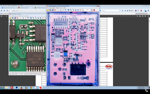
- High-resolution scanning or X-ray imaging to reveal internal layers
- Data extraction to create Gerber, netlist, and schematic files
- Verification of functionality using simulation and physical testing
- Optional prototype manufacturing and validation
Throughout the process, engineers use specialized software and manual expertise to ensure the reverse-engineered data matches the original functionality 100%.
HCFC clean solvent and it is characteristic:
It is easy to vaporize and can be decompound in the air which will bring the least damage to the ozone layer, which belongs to a interim product for printed circuit board reverse engineering, and has been regulated to phase out before 2040, so we don’t recommend this kind of cleaning solvent for pcb reverse engineering.
By using Printed Circuit Board Reverse Engineering Technology, companies can:
- Extend the life cycle of legacy systems
- Reduce operational costs and avoid complete redesigns
- Maintain independence from OEMs
- Enable redevelopment and system upgrades
- Preserve intellectual property and technical knowledge
There are two obvious problems exist for this product: one is because it is an interim product and it will bring damage to the ozone layer which can only be used till 2040, second point is the relative high cost and weak cleaning ability which can greatly increase the cleaning cost.