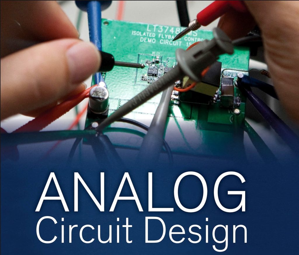
Printed Circuit Board Reverse Engineering Analog Circuit Ground
PC Board Reverse Engineering Analog Circuit Ground is an important part of PCB layout, not only because it will greatly affect the performance of electronic device but also the whole electrical emulation in the test stage;

Reverse engineering PCB card has become a commonly used technology in the electronic industry, and nowadays, printed circuit board is not long possess the single functionality circuit, most of them have the combination of digital circuit and analog circuit.
As a result of that, when copy pcb plate gerber file and layout them, the inter-course interference among them must be taken into consideration, especially the noise interference on the ground line.
The high frequency is the feature of digital circuit, while the strong sensitivity is for analog circuit. In the process of pcb reverse engineering, as for signal line, those ones with high frequency should keep as far away as possible from those sensible analog circuit components.
As for the ground line, there is only one connecting point on the printed circuit board lead to the exterial environment, so the common ground issue among the digital circuit and analog circuit must be settle within the prototype pwb reverse engineering.
As a matter of fact, the analog circuit and digital circuit within the printed circuit board are all separated, only in the place where the connecting terminal located will have a minor connection among them. Please be cautious, there is only one conjunction point over there. And there is also other pcb card reverse engineering project without any common ground which will be determined by the systematic design.
Tags: pcb assemble replicate,pcb board replicate,pcb card replicate,pcb replicate,pcba replicate,printed circuit board replicate,printed wiring board replicate,pwb replicate,pwba replicate

