

Printed Circuit Board Detailed Reverse Engineering
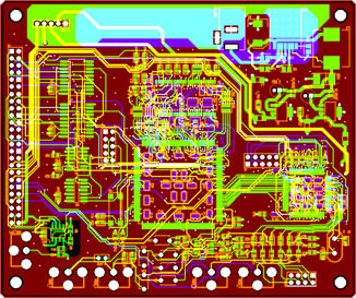
Printed Circuit Board Detailed Reverse Engineering Mainly refers to the specific circuit diagram and some specific requirements, including the mutual layout design of the PCB board and the housing, and the size of these parameters.
Next, we need to complete the reverse engineering of the entire hardware according to the guidance of the detailed design document acquired from PCB reverse engineering of the hardware module. Including schematic diagram and PCB layout drawing.
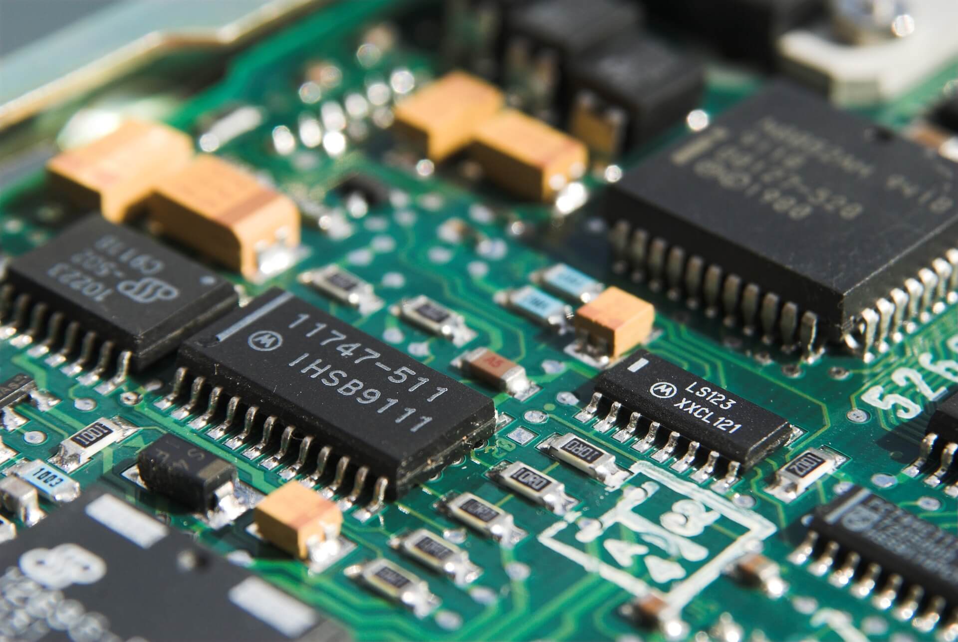
Hardware parts: Visually inspect whether there is a short circuit in the PCB board, whether the device is soldered incorrectly, or missed soldering; Test whether the resistance of each power supply to ground is normal;
Power on, test whether the power supply is normal; Debug the hardware modules by modules, with the help of oscilloscopes, logic analyzers, etc.