

Printed Circuit Board Cloning Soldering
Printed Circuit Board Cloning is a kind of technique which re-manufacture the target PCB board by extract the layout and gerber file from it;
Print the solder resist on the external layer and the layer gerber file can be drawed by cloning PCB board, then the layout part won’t be in direct contact with the electrical plating part. Silkscreen printing will be upon its surface and marking the location of each component, at the same time, it can’t cover on any layout circuit pattern or golden finger, otherwise it will decrease the solderability or the stability of current connection. Golden finger will normally be plated with gold and then insert into the extended slot to ensure the high quality of electrical current connection.
Electrical Test after manufacture PCB board according to the file from reverse engineering electronic pcb board
Test if there is any short or open circuit on the Printed circuit board, normally can use optical or electronic testing method, optical method will apply the scanning way to find out the flawless of each layer produced by the gerber file by pcb board reverse engineering, electrical test will apply flying probe test to check all of the connection. Electrical test could be more precise and accurate when spotting the short or open circuit, however, optical test can be much easier to find out the incorrect distance issue among the conductors.
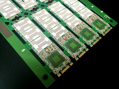
Assemble Printed circuit board
The last step is mounted and assembled electronic components on the Printed circuit board. no matter for Through hole technology or surface mount technology should use the electronic device to assemble the Printed circuit board.
Through hole technology can use the wave soldering to do the assemble, which can make all of the components be assembled onto the Printed circuit board one time. First of all, cut the lead of each component which is closed to the Printed circuit board, and bend the lead to the extent which can fix the Printed circuit board. And then transfer Printed circuit board to the water wave of solvent to make it bottom contact the soldering flux, which can help to remove the oxidation material from the bottom metal.
Tags: pcb assemble cloning,pcb board cloning,pcb card cloning,pcb cloning,pcba cloning,printed circuit board cloning,printed wiring board cloning,pwb cloning,pwba cloning