

PCBA Reverse Engineering Quality Control Documentation
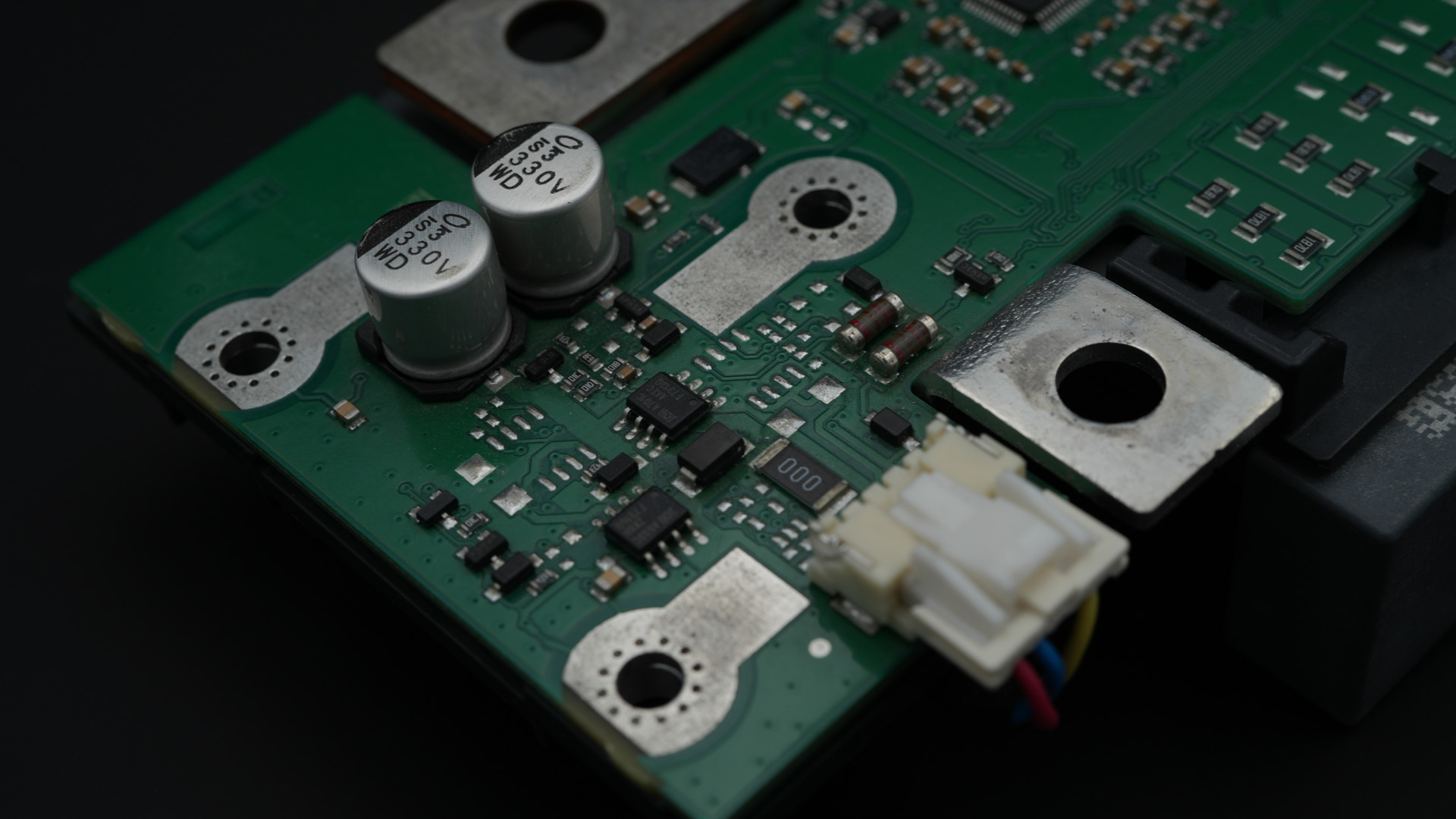
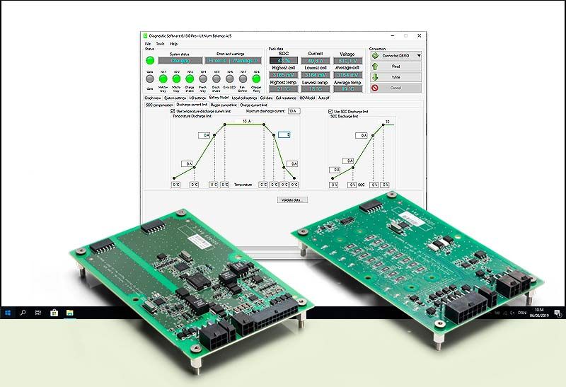
In the rapidly advancing electric vehicle (EV) industry, the Battery Management System (BMS) plays a decisive role in energy efficiency, battery protection, and safety performance. However, when the original design data or manufacturing support for these systems becomes unavailable, PCBA Reverse Engineering Quality Control Documentation becomes essential. It ensures that every step — from data recovery to remanufacture — follows strict engineering and quality standards, enabling the faithful reproduction of the original circuit board used in the BMS.
Step 1 – Recovering Design Data from the Original BMS Board
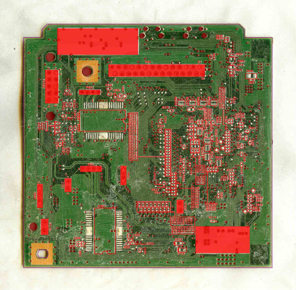
The reverse engineering process begins with detailed inspection and data recovery from the physical printed circuit board assembly (PCBA). High-resolution scanning and optical microscopy are used to map out each copper trace, via, and component footprint. From these analyses, key technical files are recreated, including:
- Gerber file – defines copper layers, solder masks, and drill data for PCB production.
- Schematic diagram – illustrates circuit logic and signal relationships for verification and redesign.
- Layout drawing – ensures mechanical accuracy for component placement.
- BOM list – identifies every part for procurement, including sensors, ICs, and MOSFETs.
- Netlist – validates interconnections between signals and helps detect missing or shorted nodes.
Together, these documents form the foundation of the PCBA Reverse Engineering Quality Control Documentation set.
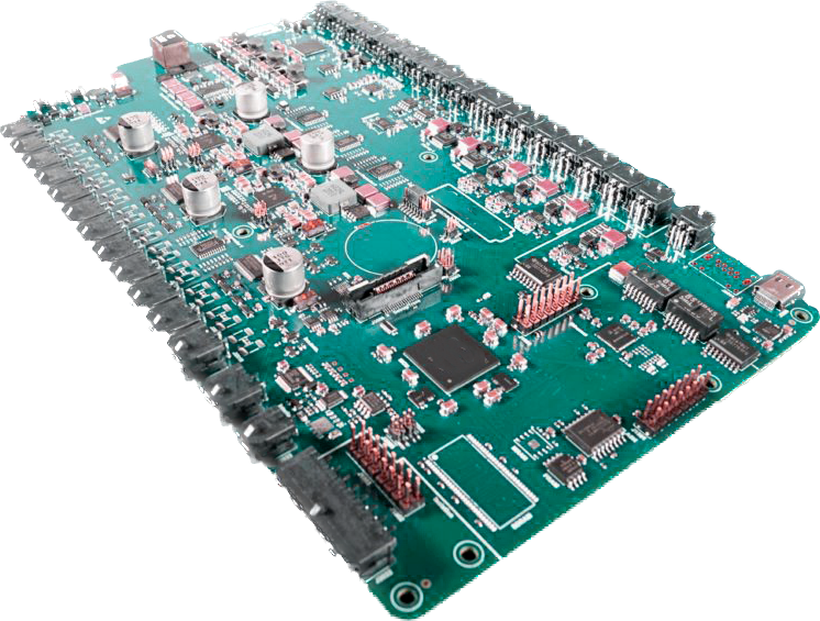
Step 2 – Bare Board Production and Component Procurement
Once documentation is verified, the Gerber file and layout drawing are sent to PCB fabrication. For BMS boards, the focus is on high-current traces, precise via alignment, and multilayer impedance control to ensure reliable thermal management and signal integrity. Meanwhile, component sourcing begins according to the BOM list. If obsolete parts are encountered, suitable replacements are carefully redeveloped or refurbished to maintain circuit equivalence.
Step 3 – Assembly and Process Validation
During assembly, each device is reproduced or replicated onto the new board using the verified layout drawing. Automated optical inspection (AOI) and X-ray imaging confirm soldering accuracy and layer alignment. For high-power BMS boards, heat dissipation zones and connector torque specifications are checked. This step integrates strict quality control documentation, ensuring that every reproduced PCBA matches the original both electrically and mechanically.
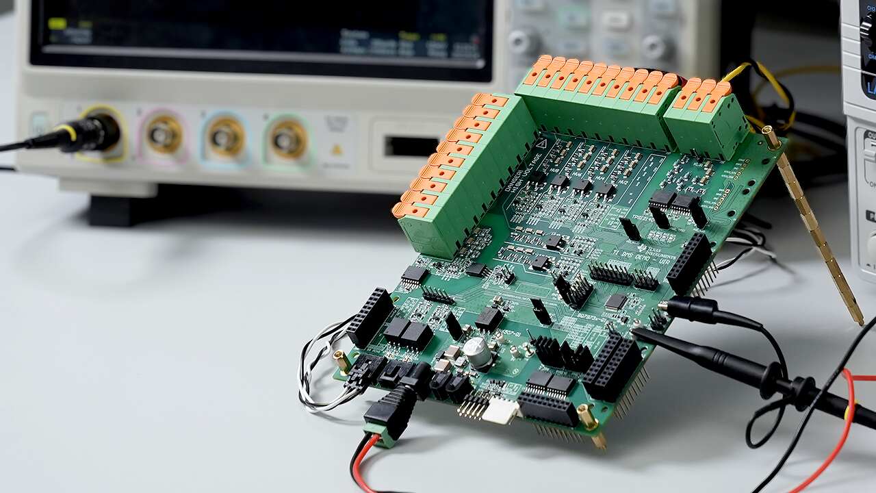
Step 4 – Functional Testing and Quality Documentation
After assembly, the reverse-engineered PCBA is tested under operational conditions. Engineers perform voltage balancing, current measurement, communication protocol verification, and temperature feedback simulation. The results are logged into the quality control documentation, forming a complete history of traceability for every remanufactured or recreated unit. This documentation includes:
- Inspection reports of layer integrity and copper uniformity.
- Test results comparing measured data with schematic expectations.
- Component certification reports confirming BOM compliance.
Such detailed records ensure that every duplicated board meets original functionality and safety standards.
Step 5 – Conversion from Reverse Engineering Data to Production
Turning reverse-engineered data into full-scale manufacturing requires disciplined management. The Gerber files and netlist must align precisely to avoid mismatched connections, and the BOM list must be constantly updated to reflect supply chain realities. Engineers should also pay attention to the redesign tolerance of high-current circuits and ensure that the layout supports long-term reliability under EV operational stress.
PCBA Reverse Engineering Quality Control Documentation include the Gerber file, layout drawing, schematic diagram and BOM list, these documents must be preserved in a more secured to ensure the security of these datas;
4th point is Rejection criteria of PCBA reverse engineering china: The rejection criteria should be determined and all discrepancies should be resolved and corrected prior to final approval of the drawings and specifications.
PCBA Reverse Engineering Quality Control Documentation transforms the reverse engineering process from a simple replication task into a complete, traceable production system. From recovering technical files to remanufacturing verified assemblies, this approach ensures that every BMS PCBA for electric vehicles can be reproduced, validated, and documented with precision. Ultimately, it guarantees that reverse-engineered boards not only match the originals but also meet the demanding quality and safety expectations of the modern EV industry.
Circuit Engineering Company Limited provide a complete PCB Reverse Engineering, PCB Clone and PCB Restoration service, Rapid Prototyping and functional test services using the latest technologies combined with traditional skills for a wide range of industries. By integrating our traditional skills with the latest technologies, we can offer clients a comprehensive portfolio of product development services all under one roof. For more details please contact our customer service team.
Tags: odgięty płytka drukowana layout,odgięty płytka drukowana part list,odgięty płytka drukowana schematic,rigid flex pcba reverse engineering,single side pcba reverse engineering