

PCB Reverse Engineering Tutorial
Reverse engineering a UAV (Unmanned Aerial Vehicle) drone PCB is a complex but essential process for replicating, modifying, or improving existing drone electronics. It involves analyzing, extracting, and reconstructing the PCB design to understand its schematic diagram, layout, and functionality. This tutorial provides a step-by-step guide to UAV drone PCB reverse engineering, covering key techniques such as component identification, layer inspection, and circuit tracing.
Step 1: PCB Preparation and Initial Inspection
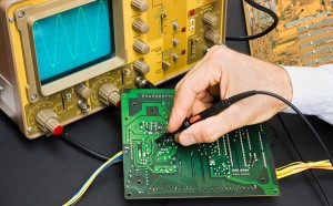
Before starting the reverse engineering process, a detailed inspection of the UAV drone PCB is required.
Visual Examination: Identify key components, connectors, and mounting positions on the board.
PCB Cleaning: Remove dust, corrosion, or protective coatings that could interfere with data extraction.
Layer Count Estimation: Check whether the board is single-layer, double-layer, or multilayer by inspecting its edge profile and vias.
Step 2: Component Identification and BOM Extraction
The next step is to identify and document all electronic components on the PCB.
Desoldering Critical Components: Carefully remove and inspect ICs, capacitors, resistors, and transistors.Marking Reference Designators: Label each component for easier schematic reconstruction.
BOM (Bill of Materials) Compilation: List component names, values, and specifications for sourcing replacements or modifications.
IC Decapsulation (if necessary): If proprietary microcontrollers or encryption ICs are present, advanced chip-level analysis may be required.
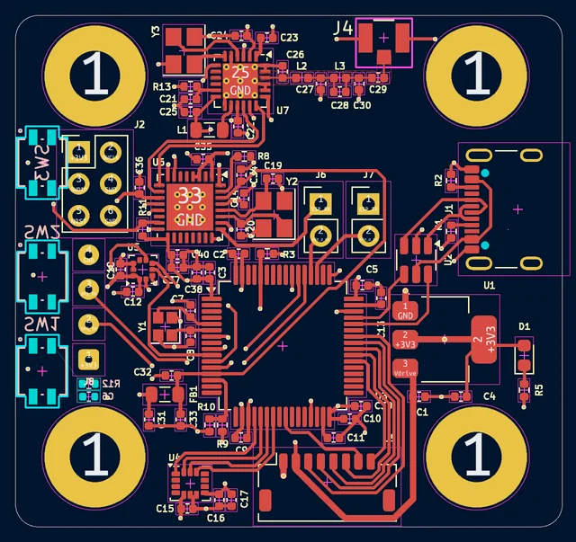
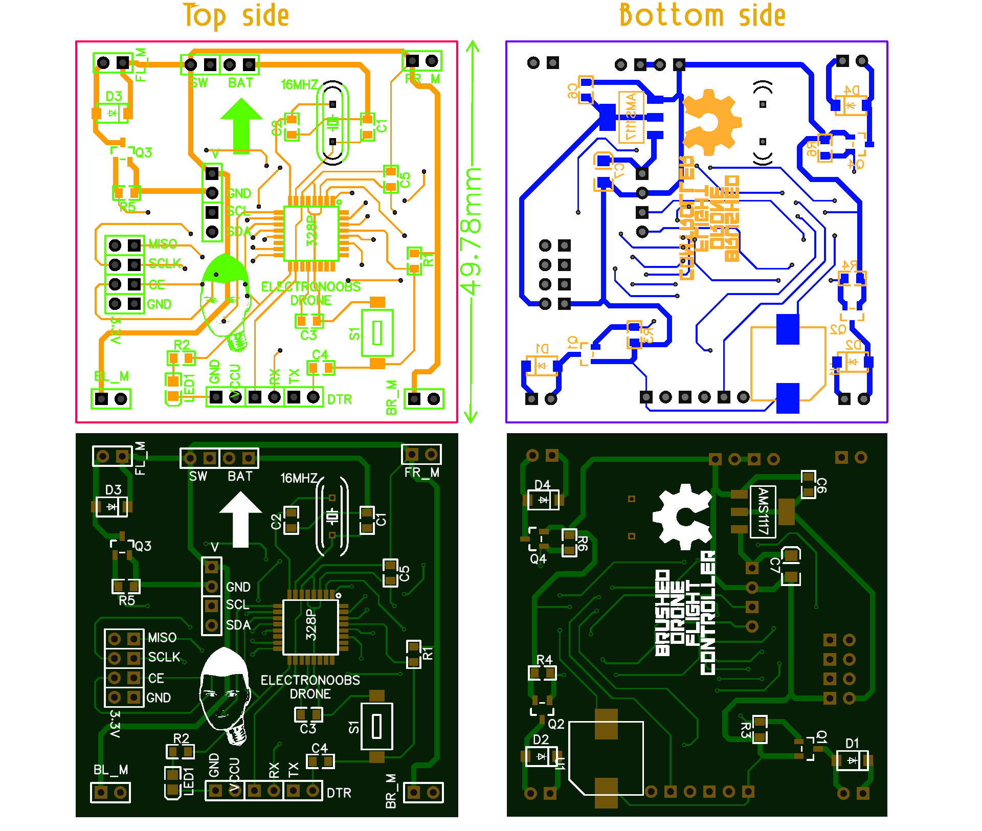
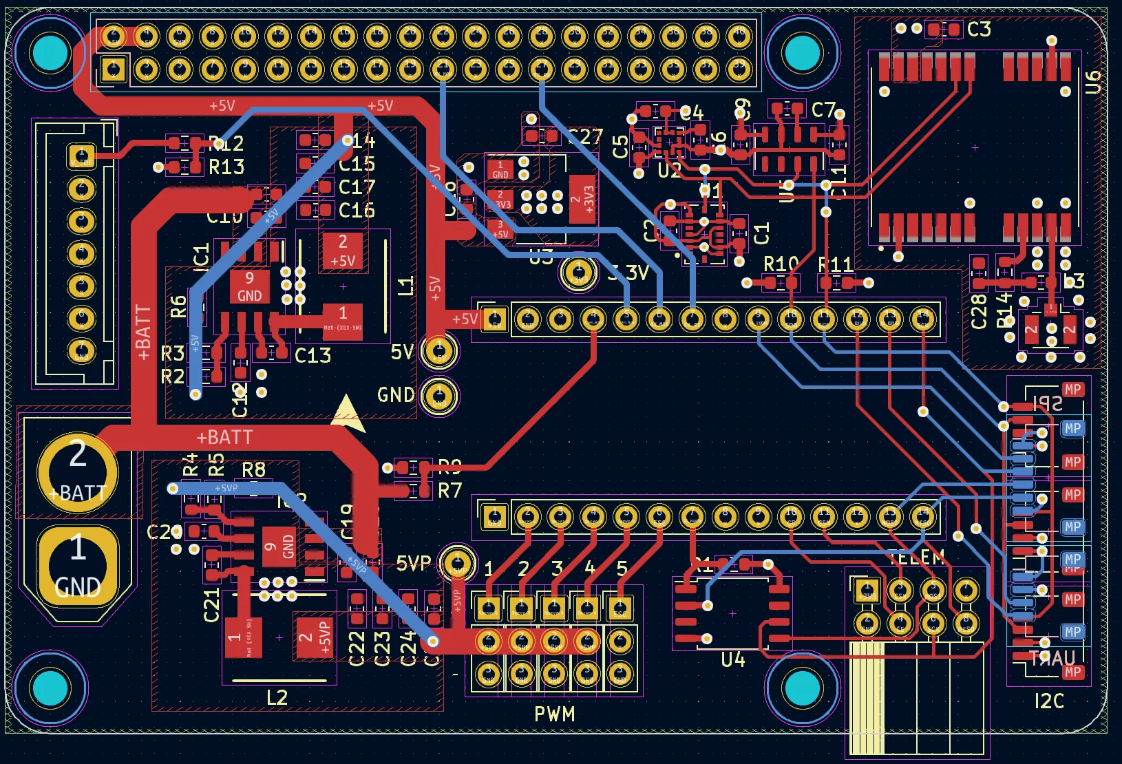
Step 3: PCB Layer and Track Tracing
Since drone PCBs are often multilayer with dense track routing, accurately mapping their connections is crucial.
High-Resolution Scanning: Capture both sides of the PCB for digital reference.X-ray Inspection for Hidden Layers: Used for BGA (Ball Grid Array) components and buried vias.Copper Trace Exposure: If needed, remove solder mask using chemical or mechanical etching to reveal circuit paths.Manually Tracing the Netlist: Identify power planes, ground connections, and signal routing.
Step 4: Schematic Diagram Reconstruction
After tracing the PCB connections, the next step is to redraw the circuit schematic using CAD software.
Use PCB Design Software: Tools like Altium Designer, Eagle, or KiCad help to digitize schematics.
Define Functional Blocks: Separate power supply, motor control, communication modules, and sensor interfaces.
Compare with Industry Standards: Validate against known drone PCB designs to ensure accuracy.
Step 5: Prototype and Testing
Once the schematic and PCB layout are recreated, it’s time to fabricate and test a prototype.
PCB Manufacturing: Generate Gerber files and send them to a PCB manufacturer.
Assembly and Soldering: Populate the board with identified components.
Functional Testing: Validate signal integrity, power management, and communication protocols to ensure the design functions correctly.
Conclusion
Reverse engineering a UAV drone PCB requires a structured approach involving inspection, component extraction, track tracing, and schematic reconstruction. By following this tutorial, engineers can successfully analyze, modify, and reproduce UAV electronics for research, repair, or optimization. At Circuit Engineering Co., LTD, we offer professional UAV PCB reverse engineering services, ensuring high precision and efficiency in drone electronics replication and development.
As par of the operation of PCB Reverse Engineering Tutorial, Functional analysis is required prior to further movement, A Functional Analysis should be accomplished to collect available documentations include the manual instruction, engineer or user notebook which can help us get clear idea about each details of the pcb we intend to reverse engineering and how it perform the function normally.
During this process, missing data is inevitable due to different reasons such as the extreme long age product, and insurficient information due to the product feature itself, at this point we need to determine all the missing data requirements, determine testing requirements because the long and order procedures go through whole each step of pcb reverse engineering service , and only after all of these information mentioned can be collected and executed properly, it would make sense to develop the pcb reverse engineering cost-estimates and schedules.
Tags: pcb plate reverse engineering,printed wiring board reverse engineering