

PCB Reverse Engineering Testing Accuracy
PCB Reverse Engineering Testing Accuracy will be depends on the preciseness of extracted layout drawing and Gerber file, and then the manufacturing capability which include facilities for PCB production and inspection;
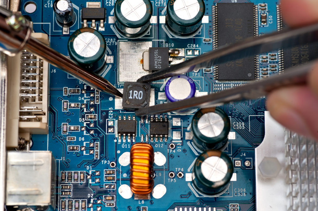
Accuracy will be dependent on probes and structure if PCB card cloning. The best case accuracy that can be expected is ±8 ps/in for the recommendations below.
If space permits, the above approach can be improved by inserting a third test structure of different length than the other two. To calculate the velocity, graph length vs. velocity with a line drawn connecting the three points. Using a least squares method, the intercept of the line with the axis gives the measurement error.
Improved accuracy propagation delay measurements can be completed with the TDR used in TDT mode. In TDT mode, probes are placed at each end of the test structure. A pulse is injected into one end and captured at the other end.
This approach has less edge-rate degradation than the simpler TDR approach, resulting in improved accuracy. Real results should only be completed with microprobes. A proper setup can achieve within ±2 ps/in accuracy when PCB Reverse Engineering decoupling.
· Traces should follow the guidelines described for impedance coupons in section 3.1.1.
· Measurement structures are defined in pairs for each signal layer, differing only in length. The recommended minimum trace lengths listed below are based on the time required for the TDR pulse to settle. The settling time will vary depending on the impedance of the trace.
· Stripline structures using microprobes should have a via at each end to route external traces for probing. The via size should be no larger than a 25 mil pad with 10 mil finished hole in the process of SMT PCB Reverse Engineering.
Tags: pcb assemble reverse engineering,pcb board reverse engineering,pcb card reverse engineering,pcb reverse engineering,pcba reverse engineering,Printed Circuit Board Reverse Engineering,printed wiring board reverse engineering,pwb reverse engineering,pwba reverse engineering