

PCB Reverse Engineering Process
The PCB reverse engineering process involves multiple critical steps, with testing and validation being one of the top priorities. Ensuring that a reverse-engineered PCB meets the required functional, structural, and reliability standards is essential before it can be reproduced or integrated into a system. This article outlines the key aspects of the testing process, including initial inspection, test plan development, and final verification procedures.

1. Initial Inspection and Hardware Evaluation
Before beginning the reverse engineering process, a thorough initial inspection of the provided PCB hardware is essential. This includes:
- Assessing the PCB’s physical condition for signs of damage, oxidation, or missing components.
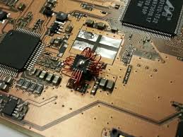
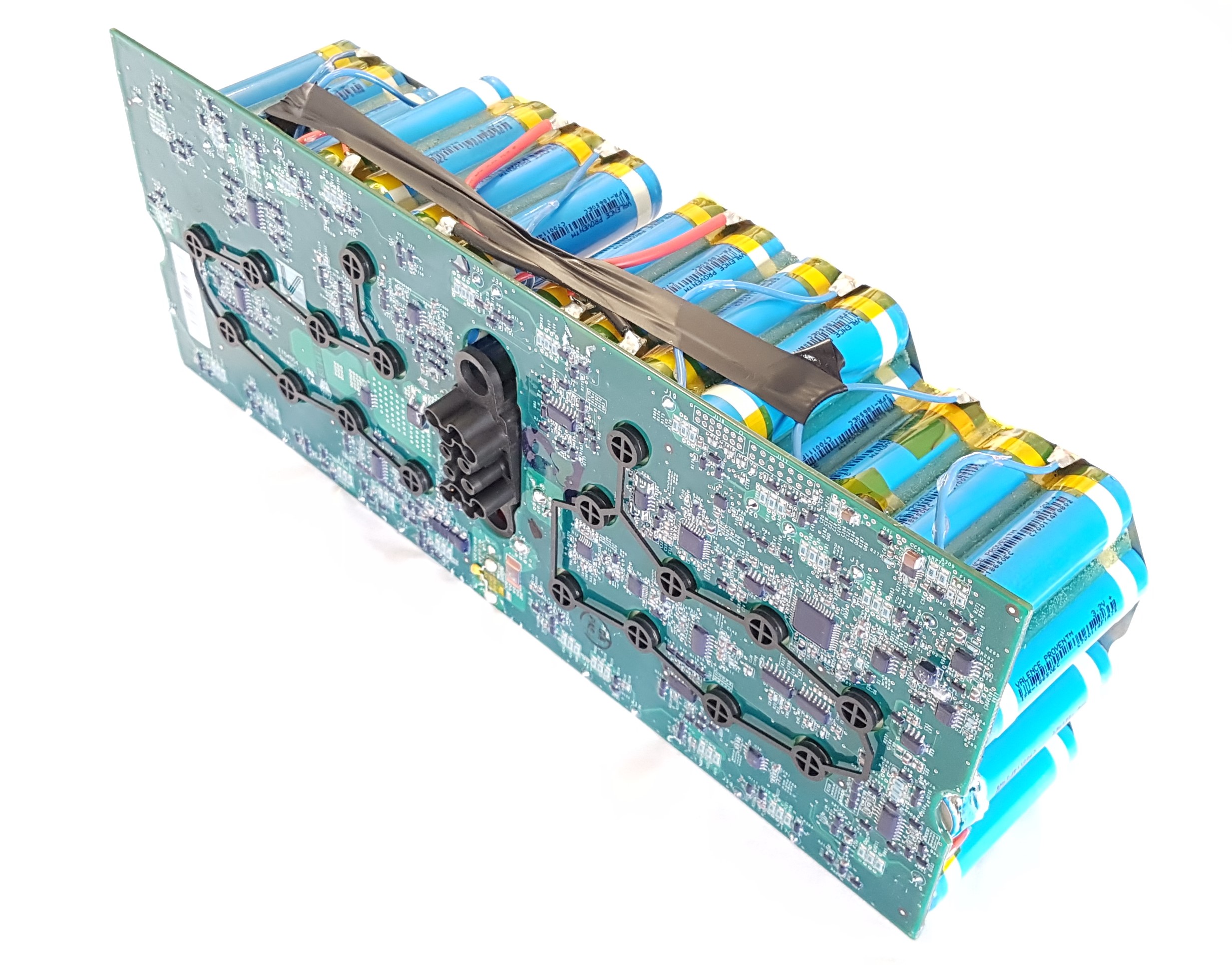
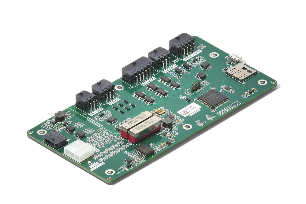
- Examining PCB complexity, including layer count, trace density, and component types (e.g., BGAs, SMDs, or through-hole components).
- Verifying power and signal connections to determine circuit functionality.
- Identifying proprietary or custom ICs, which may require additional testing or replacement.
The acceptance criteria for the prototype to be built and tested should also be established at this stage, ensuring the PCB will conform to the necessary technical specifications.
2. Development of a Standardized Test Plan
A well-defined test plan serves as the foundation for the entire PCB reverse engineering testing process. This plan must include:
- Identification of special testing requirements based on the PCB’s intended application.
- Selection of test equipment and fixtures, such as oscilloscopes, logic analyzers, thermal imaging, and X-ray inspection for multilayer boards.
- Specification of electrical testing procedures, including continuity tests, impedance analysis, and signal integrity verification.
- Environmental stress testing, if required, to assess the PCB’s performance under extreme conditions like temperature fluctuations, vibrations, and humidity.
3. Functional Testing and Performance Verification
The objective of testing in PCB reverse engineering is to ensure the replicated board functions identically to the original. This includes:
- Power-on testing to confirm proper voltage levels and component activation.
- Functional circuit verification to check the behavior of critical sections such as power regulation, data processing, and communication modules.
- Endurance testing to evaluate the long-term reliability of the reverse-engineered PCB under continuous operation.
4. Structural Integrity and Compliance Verification
Beyond electrical performance, the mechanical and structural integrity of the PCB must be tested.
- X-ray or ultrasonic testing can be used to verify hidden solder joints, BGA connections, and inner layer traces.
- Material analysis ensures that the PCB meets industry standards for heat resistance, flexibility, and durability.
- Comparison with applicable industry standards such as IPC-6012 for PCB fabrication and IPC-A-610 for assembly quality guarantees that the reverse-engineered PCB adheres to regulatory guidelines.
Conclusion
Testing is a critical phase in the PCB reverse engineering process, ensuring that the reverse-engineered design is functionally accurate, structurally sound, and reliable for real-world applications. By implementing a comprehensive test plan, engineers can verify circuit performance, identify potential design flaws, and optimize the PCB for improved functionality. We specialize in high-precision PCB reverse engineering services, ensuring that all recreated designs meet the highest quality and reliability standards.
Tags: pcb card reverse engineering,pwb reverse engineering