"Everything we build starts with design engineering. CECL manufactured boards for one of our products. It went perfectly – a real success.It is really an high quality service they have provided to us!"
By Nile Smith from Sinotech Inc.
“We had several very old device with obsolete boards need to be replaced –through CECL professional service.We got what we needed, and we’ve been using the results of the work without any problem till now.”
By Richard Anderson from TWP system Inc.
"Guys from CECL manufacture PCBs we use in one of our products, a clinometer and we’ve never had a problem with anything. The boards come in, they work. And, their team is very responsive."
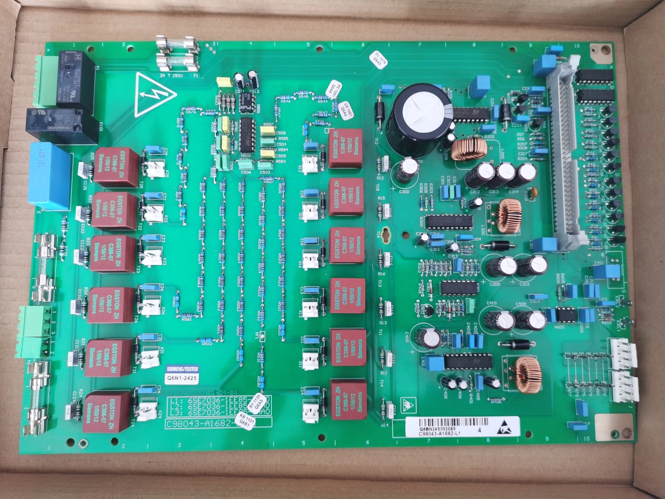
Ingenieure zerlegen und scannen jede Lage der Leiterplatte sorgfältig, um präzise Schaltpläne, Netzlisten, Layoutzeichnungen und Gerber-Dateien zu erstellen. Mithilfe hochauflösender Bildgebung und elektrischer Messungen ermittelt das Team die exakte Leiterbahnführung von Gleichtakt-Drosseln, X- und Y-Kondensatoren, Gleichrichterbrücken und Überspannungsschutzkomponenten. Die Stückliste wird Bauteil für Bauteil neu erstellt, wobei Spannungsfestigkeit, Toleranzen und thermische Klassifizierungen überprüft werden. Während dieser Reverse-Engineering-Phase erstellen die Spezialisten außerdem eine vollständige CAD-Datei und eine Bestückungsplandatei, um die Kompatibilität mit der Produktion sicherzustellen. Jede aus den Leiterbahnen extrahierte Netzliste wird mit dem rekonstruierten Schaltplan abgeglichen, um Abweichungen vor dem Klonen oder Duplizieren der Leiterplatte zu vermeiden. Die Erstellung einer validierten Gerber-Datei ist kein einfacher Kopiervorgang; sie erfordert die genaue Messung von Leiterbahnbreite, Kriechstrecken, Isolationsschlitzen und Masseflächen, um die Wirksamkeit der EMV-Filterung zu gewährleisten. Dank dieses systematischen Vorgehens können die Ingenieure die Leiterplatte mit identischem elektrischem Verhalten zuverlässig reproduzieren.
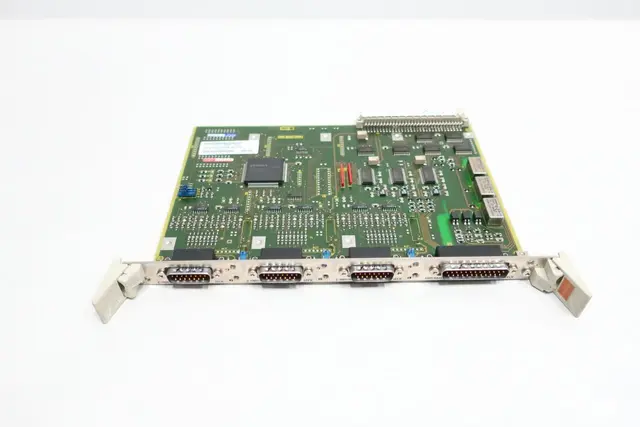
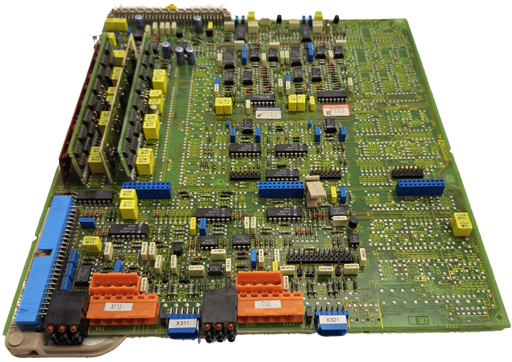
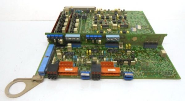
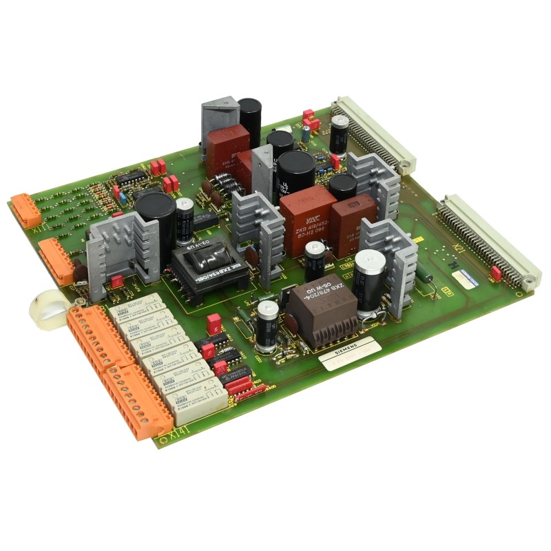
Cloning a line noise PCB for the Siemens Simodrive power supply requires a highly controlled reverse engineering methodology, especially because this board plays a critical role in electromagnetic interference suppression and power stability. The line noise PCB is responsible for filtering conducted emissions, stabilizing DC bus input, and protecting downstream drive modules from voltage spikes. When initiating a reverse engineering project on this Siemens Simodrive power supply assembly, engineers must first evaluate electrical topology, grounding architecture, and filtering stages. The objective is not simply to copy copper traces, but to recover the original filtering characteristics, restore impedance balance, and recreate safety compliance performance. A structured plan ensures that every step—from documentation extraction to reproduce validation—supports reliable remanufacture and long-term operational stability.
Mühendisler, doğru şematik diyagram, netlist, yerleşim çizimi ve Gerber dosya verilerini oluşturmak için PCB’nin her katmanını dikkatlice söküp tarar. Yüksek çözünürlüklü görüntüleme ve elektriksel problama kullanarak, ekip ortak mod bobinlerinin, X ve Y kapasitörlerinin, doğrultucu köprülerinin ve aşırı gerilim bastırma bileşenlerinin hassas yönlendirmesini kurtarmak için çalışır. Malzeme listesi, voltaj değerlerini, tolerans seviyelerini ve termal sınıflandırmaları doğrulayarak bileşen bileşen yeniden oluşturulur. Bu tersine mühendislik aşamasında, uzmanlar ayrıca üretim uyumluluğunu sağlamak için eksiksiz bir CAD dosyası ve yerleştirme yönlendirme dosyası oluşturur. Bakır izlerinden çıkarılan her netlist, kartı kopyalamaya veya çoğaltmaya çalışmadan önce tutarsızlıkları önlemek için yeniden oluşturulan şematik diyagrama karşı çapraz doğrulanır. Doğrulanmış bir Gerber dosyası oluşturmak basit bir kopyalama işlemi değildir; EMI filtreleme etkinliğini korumak için iz genişliğinin, kaçak mesafesinin, izolasyon yuvalarının ve topraklama düzlemlerinin dikkatli bir şekilde ölçülmesini gerektirir. Bu disiplinli yaklaşım sayesinde, mühendisler PCB’yi aynı elektriksel davranışla güvenle yeniden üretebilirler.
Siemens Simodrive Power Supply Line Noise PCB Clone can reproduce a printed circuit board in the precontext of all the productive documents are absent by extract layout, gerber file and schematic from existing PCB board
PCB Clone will inevitably encounter the noise issue from power supply line, when the emergence of electro-magnetic interference on the digital circuit, the main reason is on the power supply line and grounding line, use oscillograph to monitor the obvious noise voltage. Although there are a lot of people can assure that these noises is the main cause for electro-magnetic interference when restore wiring diagram from PCB, but normally has no effective measures to deal with them, in order to achieve the purpose of noise elimination, it is necessary to understand the generating source of these noises:
Gli ingegneri smontano e scansionano attentamente ogni strato del PCB per generare diagrammi schematici, netlist, disegni di layout e dati del file Gerber accurati. Utilizzando immagini ad alta risoluzione e sonde elettriche, il team lavora per recuperare il routing preciso di induttori di modo comune, condensatori X e Y, ponti raddrizzatori e componenti di soppressione delle sovratensioni. La distinta base viene ricostruita componente per componente, confermando tensioni nominali, livelli di tolleranza e classificazioni termiche. Durante questa fase di reverse engineering, gli specialisti creano anche un file CAD completo e un file di orientamento pick&place per garantire la compatibilità di produzione. Ogni netlist estratta dalla tracciatura in rame viene verificata incrociata con lo schema elettrico ricreato per evitare discrepanze prima di tentare di clonare o duplicare la scheda. Generare un file Gerber convalidato non è un semplice processo di copia; richiede un’attenta misurazione della larghezza della traccia, della distanza di dispersione, degli slot di isolamento e dei piani di messa a terra per mantenere l’efficacia del filtraggio EMI. Grazie a questo approccio disciplinato, gli ingegneri possono riprodurre con sicurezza il PCB con un comportamento elettrico identico.
1, noise from the power supply line:
From the graphic below, there is a typical gate circuit output terminal, when the output is high electrical level, Q3 is open circuit, Q4 cut out; when the output is low electrical level, Q3 cut out, and Q4 is open circuit. Both these two status can form the high impedance value, which can restrict the current from power supply.
When the status of PCB circuit change, Q3 and Q4 will bring to connection together in a transient moment, and this moment there will be a transient low impedance value occurs between the power supply and ground, it will generate like 30-100mA peak value current.
Les ingénieurs démontent et scannent minutieusement chaque couche du circuit imprimé afin de générer un schéma précis, une netlist, un plan d’implantation et un fichier Gerber. Grâce à l’imagerie haute résolution et au sondage électrique, l’équipe s’attache à reconstituer le routage précis des inductances de mode commun, des condensateurs X et Y, des ponts redresseurs et des composants de protection contre les surtensions. La nomenclature est reconstruite composant par composant, en vérifiant les tensions nominales, les tolérances et les classifications thermiques. Au cours de cette phase de rétro-ingénierie, les spécialistes créent également un fichier CAO complet et un fichier d’orientation pour le placement des composants afin de garantir la compatibilité avec la production. Chaque netlist extraite des pistes de cuivre est vérifiée par rapport au schéma reconstitué afin d’éviter toute incohérence avant toute tentative de clonage ou de duplication de la carte. La génération d’un fichier Gerber validé ne se limite pas à une simple copie ; elle exige une mesure précise de la largeur des pistes, des distances de fuite, des fentes d’isolation et des plans de masse afin de maintenir l’efficacité du filtrage EMI. Grâce à cette approche rigoureuse, les ingénieurs peuvent reproduire le circuit imprimé avec un comportement électrique identique.
And when the gate output electrical level turns from low to high, power supply will not only keep the output current, but also charge the capacitor which makes the current value reach saturation. Due to there is different level of conductance value on the power supply line when clone pcb card, as a result of that, when current start to muted, sensible voltage will emerge. And the noise on the power supply line can be monitored. Also due to the existence of power supply line impedance, the voltage will fall in the short time.
Component validation and signal integrity testing form the second dense technical stage of the cloning process. Once the schematic diagram and bom list are restored, engineers simulate filtering performance to confirm that recreated circuits meet original attenuation specifications. Reverse engineering includes evaluating magnetic core materials in chokes, ESR values of capacitors, and discharge resistor placement to ensure compliance with industrial safety standards. If obsolete components are discovered, controlled redesign or redevelopment may be required to maintain equivalent filtering bandwidth and thermal stability. During this stage, the layout drawing is refined to optimize current loops and minimize parasitic inductance without altering functional topology. Updated cad file data and pick&place orientation file outputs are generated to support automated assembly. Before remanufacture begins, prototype boards are fabricated using the recovered Gerber file and validated against original power supply modules to confirm identical suppression characteristics. Only after thorough electrical comparison can the clone or replicate version be approved for scaled production.
इंजीनियर PCB की हर लेयर को ध्यान से अलग करते हैं और स्कैन करते हैं ताकि सही स्कीमैटिक डायग्राम, नेटलिस्ट, लेआउट ड्राइंग और Gerber फ़ाइल डेटा बनाया जा सके। हाई-रिज़ॉल्यूशन इमेजिंग और इलेक्ट्रिकल प्रोबिंग का इस्तेमाल करके, टीम कॉमन-मोड चोक, X और Y कैपेसिटर, रेक्टिफायर ब्रिज और सर्ज सप्रेशन कंपोनेंट की सटीक रूटिंग को रिकवर करने के लिए काम करती है। BOM लिस्ट को कंपोनेंट दर कंपोनेंट फिर से बनाया जाता है, जिससे वोल्टेज रेटिंग, टॉलरेंस लेवल और थर्मल क्लासिफिकेशन कन्फर्म होते हैं। इस रिवर्स इंजीनियरिंग फेज़ के दौरान, स्पेशलिस्ट प्रोडक्शन कम्पैटिबिलिटी पक्का करने के लिए एक पूरी CAD फ़ाइल और पिक एंड प्लेस ओरिएंटेशन फ़ाइल भी बनाते हैं। कॉपर ट्रेसिंग से निकाली गई हर नेटलिस्ट को बोर्ड को क्लोन या डुप्लिकेट करने की कोशिश करने से पहले, किसी भी गड़बड़ी से बचने के लिए फिर से बनाए गए स्कीमैटिक डायग्राम से क्रॉस-वेरिफाई किया जाता है। एक वैलिडेट Gerber फ़ाइल बनाना कोई आसान कॉपी प्रोसेस नहीं है; इसके लिए EMI फ़िल्टरिंग इफेक्टिवनेस बनाए रखने के लिए ट्रेस की चौड़ाई, क्रीपेज दूरी, आइसोलेशन स्लॉट और ग्राउंडिंग प्लेन को ध्यान से मापने की ज़रूरत होती है। इस डिसिप्लिन्ड अप्रोच से, इंजीनियर आत्मविश्वास से एक जैसे इलेक्ट्रिकल बिहेवियर के साथ PCB को रीप्रोड्यूस कर सकते हैं।
The final phase focuses on production readiness and lifecycle sustainability for the Siemens Simodrive power supply line noise PCB. After engineers successfully restore documentation and reproduce validated prototypes, the complete data package—including schematic diagram, netlist, bom list, layout drawing, cad file, pick&place orientation file, and Gerber file—is standardized for manufacturing control. Quality assurance procedures verify solder joint integrity, isolation spacing, and thermal performance under continuous industrial load. Refurbish strategies may also be applied to extend the lifespan of legacy modules while maintaining compatibility with existing Simodrive systems. By combining systematic reverse engineering, precision documentation recovery, and controlled redesign where necessary, companies can confidently duplicate and remanufacture line noise PCBs for industrial drive applications. This comprehensive cloning approach not only ensures electrical reliability and EMI compliance but also strengthens technical documentation assets, enabling sustainable redevelopment and efficient global production support.