

PCB Circuit Card Reverse Engineering for Drawing and Removing Basic Objects
PCB Circuit Card Reverse Engineering is a process through which the electronic printed circuit board’s productive documents can be made include the Gerber file, layout drawing, BOM file and schematic diagram can be acquired;
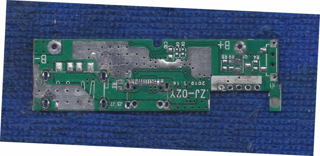
There are several ways of PCB card clone and creating new objects: you can draw them yourself, you can copy an existing object (or selection), or you can load an element from a file or from the Library window. Each type of object has a particular tool for creating it.
The active tool can be selected from the tool selectors in the bottom left corner or by one of the function keys listed earlier in this chapter. Each <Btn1> press with the tool tells the application to create or change the appropriate object or at least take the first step to do so before PCB wiring card clone.
Each tools causes the cursor to take on a unique shape and also causes the corresponding tool selector button to be highlighted. You can use either cue to see which tool is active. The button labeled ‘Sel Net On Layout’ can be used to select (on the layout) everything that is connected (or is supposed to be connected) to the net.
If you click on a connection in the connection list, it will select/deselect the corresponding pin or pad in the layout and also center the layout window where it is located. If you “Find” (‘lookup connection to object’ in the Connects menu [also F key]), a pin or pad it will also choose the net and connection in the netlist window if it exists in the netlist.
If no netlist exists for the layout, then the netlist window does not appear. You can load a netlist from a file from the File menu after Reverse Engineering electronic circuit board. The format for netlist files is described in Section 7.5 [Netlist File], page 60.
Tags: copying pcb circuit card artwork,copying pcb circuit card bom,copying pcb circuit card component list,copying pcb circuit card design,copying pcb circuit card diagram,copying pcb circuit card drawing,copying pcb circuit card gerber file,copying pcb circuit card layout,copying pcb circuit card part list,copying pcb circuit card schematic