

PCB Board Reverse Engineering Subsystem
PCB Board Reverse Engineering Subsystem
In the process of pcb board reverse engineering, Any subsystem or circuit layout operating at high frequency and/or high precision with both analog and digital signals should like to have those signals physically separated as much as possible to prevent crosstalk. This is typically difficult to accomplish in practice.
Crosstalk can be minimized by paying attention to the system layout and preventing different signals from interfering with each other after reverse engineering pcb board. High level analog signals should be separated from low level analog signals, and both should be kept away from digital signals. TTL and CMOS digital signals have high edge rates, implying frequency components starting with the system clock and going up form there. And most logic families are saturation logic, which has uneven current flow (high transient currents) which can modulate the ground from pcb board reverse engineering. We have seen elsewhere that in waveform sampling and reconstruction systems the sampling clock (which is a digital signal) is as vulnerable to noise as any analog signal. Noise on the sampling clock manifests itself as phase jitter, which as we have seen in a previous section, translates directly to reduced SNR of the sampled signal. If clock driver packages are used in clock distribution, only one frequency clock should be passed through a single package. Sharing drivers between clocks of different frequencies in the same package will produce excess jitter and crosstalk and degrade performance after pcb board reverse engineering.
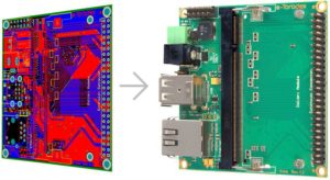
The ground plane can act as a shield where sensitive signals cross. Figure 12.1 shows a good layout for a data acquisition board where all sensitive areas are isolated from each other and signal paths are kept as short as possible. While real life is rarely as simple as this, the principle remains a valid one from PCB REVERSE ENGINEERING.