

PCB Board Reverse Engineering Process
PCB Board Reverse Engineering Process
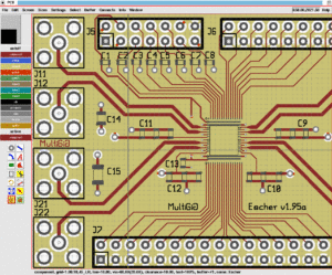
In the PCB Board reverse engineering process, layout is a very critical step for the final product completion, in other words, all the works and preparation made in previous steps are all for it, the restriction and limitation on the layout process is the strictest one, and dedicate techniques with great amount of workload need to be implemented.
PCB Board reverse engineering will have single side, double side and multilayer layout; and the methods of layout will be categorized as two ways: Automatic and interactive way:
PCB Board Reverse Engineering Process
Before the execution of automatic layout, interactive method can be used in advance, layout PCB board wires with higher requirement and more restriction, input terminal and output terminal’s sideline must avoid to be layout in the parallel way to prevent the reflection interference.
And the ground isolation can be added, the tracks on the adjacent layers should be vertically layout since the parallel way cause parasite coupling;