

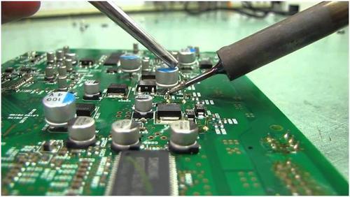
PC Board Reverse Engineering Layout
PC Board Reverse Engineering Layout must be inspected before enter the Printed circuit board re-manufacturing stage to ensure the layout drawing and gerber file which has been generated will be exactly the same as original PC board;
After the completion of PC Board Reverse engineering and component layout, it is time to start the layout of circuit pattern. The basic principle of Layout for the purpose of PC Board Reproduction is: spare no effort to choose the layout design with the lowest density in the condition of assembly density allowance, at the same time, signal pattern layout must has the same width and space to facilitate the impedance matchment.
Regarding to radio frequency circuit, the unreasonable design of orientation, width and space of signal tracks, will probably cause the cross interference with signal transmitting lines; beside, there is noise interference embedded inside the systematic power supply itself, as a result of that, when Reverse engineering PCB Board, engineer must take the comprehensive consideration into account for reasonable layout.
When layout the circuit pattern, all of the layout circuit must keep at least two millimeters distance from the frame of PC Board, to avoid the track break out or potentials of track breakout when manufacture PC Board. power supply track must be as wide as possible from recreated PC Board file to reduce the cycle circuit resistance, at the same time,
Tags: reverse engineering pcb bom,reverse engineering pcb design,reverse engineering pcb gerber,reverse engineering pcb layout,reverse engineering pcb schematic