

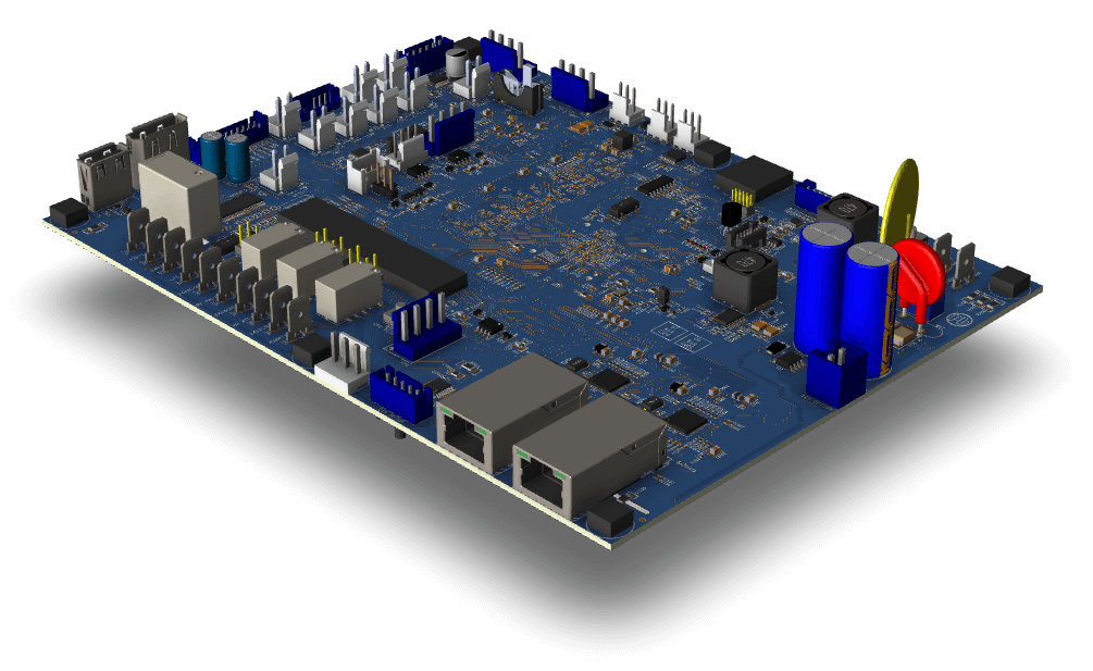
Multilayer Printed Circuit Board Reverse Engineering
Multilayer printed circuit board is constituted by over two layers of inductor (copper foil layer) press across each other. Copper foil layers are attached by the prepreg together. Multilayer printed circuit board is one of the most complicate types in the printed circuit board reverse engineering family due to the high complicate process, low production output and difficult make its cost higher than others.
High density interconnect multilayer printed circuit board caused by the increased density of integrated circuit and make it the necessity for electronic industry. In the layout process of HDI PCB Board with buried and blind vias, there are unpredictable issues during the course from noise, littered capacitor and crosstalk, etc. as a result of that, Reverse Engineering multilayer printed circuit board can help to minimize the length of copper track and avoid the parallel tracks.
Obviously, in the single side and double side PCB reverse engineering, due to the limitation of cross quantity, these issues can be solved with satisfactory. In terms of tremendous cross intersection, multilayer printed circuit board must be made if the whole functions need to be fulfilled. So the original reason for multilayer PCB board reverse engineering is provide the most possible latitude for layout route of the electronic and electric circuit.
Multilayer printed circuit board has at least three copper foil layer as the conductor, two of them on the surface and the remaining ones embedded between the insulating material. Their electrical connection is through the vias which has been metalized during the processing.
Tags: pcb assemble reverse engineering,pcb board reverse engineering,pcb card reverse engineering,pcb reverse engineering,pcba reverse engineering,Printed Circuit Board Reverse Engineering,printed wiring board reverse engineering,pwb reverse engineering,pwba reverse engineering