

Multilayer PCB Board Reverse Engineering
The Multilayer PCB Board Reverse Engineering needs to take high frequency signals back flow and it is supposed to layout on the reference ground layer which is adjacent to signal layer which will has the minimum back flow and impedance. But actually there is curve and cutout embedded inside the ground or/and power supply, which can change the route of flow back and cause the increased flow back area, consequently will cause electro-radiation and bounce back noise.
If the engineers have clear idea about the route of current then he can dramatically avoid the big flow back and control the electro-magnetic radiation. But the route of flow back can be determined by signal line layout, Multilayer PCB power supply and ground layout structure and power source point, decoupling capacitor and component placement location, etc. so it is quite difficult to estimate the flow back route in theory.
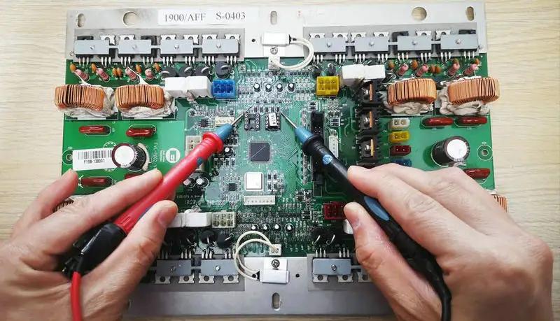
It is quite critical to eliminate the noise issue in the process of multilayer PCB board reverse engineering, we can see the signal wave shape through oscillograph and help us to solve the signal integrity issue through PCB board reverse engineering, but is there any facility can see the shape of radiation and flow back on the multilayer PCB?
Electro-Magnetic High Speed Scanning Measurement Technology:
In the method of electro-magnetic radiation measurement way, there is a near field scanning measurement to solve the problem. This method is based upon the multilayer PCB board reverse engineering principle, the electro-magnetic is generated from high frequency current flow back of being detected device. Such as EMSCAN electro-magnetic radiation scanning system made from Canada by the principle, it apply H grid array microprobe (32×40=1280 microprobes) to detect the current of DUT.
Tags: pcb assemble reverse engineering,pcb board reverse engineering,pcb card reverse engineering,pcb reverse engineering,pcba reverse engineering,Printed Circuit Board Reverse Engineering,printed wiring board reverse engineering,pwb reverse engineering,pwba reverse engineering